


 Flexible Thinking: PCB Designers Still Wanted
 Connect the Dots: Five Best Practices for Designing Flex and Rigid-flex PCBs
 Tim’s Takeaways: Human Ingenuity and the Rigid-flex PCB
Hitachi Chemical to Build New Factory in Taiwan to Manufacture Laminate Materials for PWB
April 18, 2018 | Hitachi Chemical Co., Ltd.Estimated reading time: Less than a minute
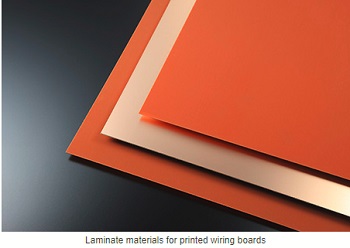
Hitachi Chemical Co., Ltd. has decided to construct a new factory to manufacture advanced functional laminate materials for printed wiring boards (pre-preg and copper-clad laminates) on the site of Hitachi Chemical Electronic Materials (Taiwan) Co., Ltd. (HCET), Hitachi Chemical's subsidiary in Taiwan. Hitachi Chemical will invest a total of approximately 7.5 billion yen and the new factory will begin operation by April 2020.
Hitachi Chemical's laminate materials for printed wiring boards are being well received in the market, especially with demand for its advanced functional laminate materials for semiconductor packaging substrates used in various fields, including 5th generation wireless systems (5G), advanced driver-assistance systems (ADAS) and artificial intelligence (AI), expected to grow stronger in the medium- to long-term. To address its customer needs promptly under these circumstances, Hitachi Chemical has decided to invest in establishing a supply system in Taiwan, the biggest demand center for advanced functional laminate materials.
Hitachi Chemical will take advantage of this new factory to boost the sales of its advanced functional laminate materials by developing a production system capable of delivering timely supplies to its customers.
Share on:


Suggested Items
The Chemical Connection: Reducing Etch System Water Usage, Part 2
05/02/2024 | Don Ball -- Column: The Chemical ConnectionIn my last column, I reviewed some relatively simple ways to reduce water usage in existing etch systems: cutting down cooling coil water flow, adding chillers to replace plant water for cooling, lowering flow rate nozzles for rinses, etc. This month, I’ll continue with more ways to control water usage in your etcher. Most of these are not easily retrofittable to existing equipment but should be given serious consideration when new equipment is contemplated. With the right combination of add-ons, it is possible to bring the amount of water used in an etch system to almost zero.
Designer’s Notebook: What Designers Need to Know About Manufacturing, Part 2
04/24/2024 | Vern Solberg -- Column: Designer's NotebookThe printed circuit board (PCB) is the primary base element for providing the interconnect platform for mounting and electrically joining electronic components. When assessing PCB design complexity, first consider the component area and board area ratio. If the surface area for the component interface is restricted, it may justify adopting multilayer or multilayer sequential buildup (SBU) PCB fabrication to enable a more efficient sub-surface circuit interconnect.
Insulectro’s 'Storekeepers' Extend Their Welcome to Technology Village at IPC APEX EXPO
04/03/2024 | InsulectroInsulectro, the largest distributor of materials for use in the manufacture of PCBs and printed electronics, welcomes attendees to its TECHNOLOGY VILLAGE during this year’s IPC APEX EXPO at the Anaheim Convention Center, April 9-11, 2024.
ENNOVI Introduces a New Flexible Circuit Production Process for Low Voltage Connectivity in EV Battery Cell Contacting Systems
04/03/2024 | PRNewswireENNOVI, a mobility electrification solutions partner, introduces a more advanced and sustainable way of producing flexible circuits for low voltage signals in electric vehicle (EV) battery cell contacting systems.
Heavy Copper PCBs: Bridging the Gap Between Design and Fabrication, Part 1
04/01/2024 | Yash Sutariya, Saturn Electronics ServicesThey call me Sparky. This is due to my talent for getting shocked by a variety of voltages and because I cannot seem to keep my hands out of power control cabinets. While I do not have the time to throw the knife switch to the off position, that doesn’t stop me from sticking screwdrivers into the fuse boxes. In all honesty, I’m lucky to be alive. Fortunately, I also have a talent for building high-voltage heavy copper circuit boards. Since this is where I spend most of my time, I can guide you through some potential design for manufacturability (DFM) hazards you may encounter with heavy copper design.