


 It’s Only Common Sense: OCCAM—the Time Is Now
 Marcy's Musings: The Growing Industry
 Dan’s Biz Bookshelf: Seeing the How
Controlling the Properties of Matter in Two-Dimensional Crystals
October 27, 2016 | Penn State Materials Research InstituteEstimated reading time: 3 minutes
By creating atomic chains in a two-dimensional crystal, researchers at Penn State believe they have found a way to control the direction of materials properties in two and three dimensional crystals with implications in sensing, optoelectronics and next-generation electronics applications ("Spontaneous formation of atomically thin stripes in transition metal dichalcogenide monolayers").
Whether an alloy has a random arrangement of atoms or one that is ordered can have large effects on a material’s properties. In a new paper published online in the journal Nano Letters, Nasim Alem, assistant professor of materials science and engineering, and colleagues at Penn State used a combination of simulations and scanning transmission electron microscopy imaging to determine the atomic structure of an ordered alloy of molybdenum, tungsten and sulfur. They determined that fluctuations in the amount of available sulfur were responsible for the creation of atomic chains of either molybdenum or tungsten.
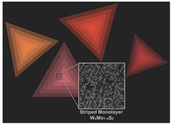
An electron microscopy image of ordered atoms of tungsten (W) and molybdenum (Mo) against artistic representations of triangular single layer flakes of WxMo1–xS2 on a substrate
An electron microscopy image of ordered atoms of tungsten (W) and molybdenum (Mo) against artistic representations of triangular single layer flakes of WxMo1–xS2 on a substrate. (Amin Azizi and Andrea Kohler/Penn State)
“We discovered how chains form in a two-dimensional alloy as a result of fluctuations in the amount of a particular precursor, in this case sulfur,” Alem said. “Normally, when we combine atoms of different elements, we don’t know how to control where the atoms will go. But we have found a mechanism to give order to the atoms, which in turn introduces control of the properties, not only heat transport, as is the case in this work, but also electronic, chemical or magnetic properties in other alloy cases. If you know the mechanism, you can apply it to arrange the atoms in a wide range of alloys in 2D crystals across the Periodic Table.”
In the case of the molybdenum, tungsten and sulfur alloy, they showed that the electronic properties were the same in every direction, but using simulations they predict that the thermal transport properties are smaller perpendicular to the chains or stripes.
“We didn’t know why this crystal forms an ordered structure, so we worked with my colleague Dr. Vin Crespi to understand the underlying physics that causes order in this crystal. Our calculations show it was the fluctuations in the third element, sulfur, that was determining how the chains formed,” Alem said.
Vincent H. Crespi, Distinguished Professor of Physics, and professor of chemistry and materials science and engineering who developed the theoretical understanding of the phenomenon, said, "Although the interior of the flake is indifferent to whether molybdenum or tungsten occupies any site in the crystal lattice, the edge of the growing crystal does care: Depending on how much sulfur is available at a given location, the edge will prefer to be either 100% molybdenum or 100% tungsten. So as the availability of sulfur randomly varies during growth, the system alternately lays down rows of molybdenum or tungsten. We think this may be a general mechanism to create stripe-like structures in 2D materials."
Amin Aziz, who is a Ph.D. candidate in Alem’s group and lead author on the Nano Letters paper, produced the STEM imaging and spectroscopy that showed the fine atomic structure of the alloy samples and their electronic properties.
“When we are able to directly image constitutive atoms of a substance, see how they interact with each other at the atomic level and try to understand the origins of such behaviors, we could potentially create new materials with unusual properties that have never existed,” said Azizi.
A team led by Mauricio Terrones, professor of physics, produced samples of this ordered alloy by vaporizing powders of all three elements, called precursors, under high heat.
Share on:


Suggested Items
SMC Korea 2024 to Highlight Semiconductor Materials Trends and Innovations on Industry’s Path to $1 Trillion
04/24/2024 | SEMIWith Korea a major consumer of semiconductor materials and advanced materials a key driver of innovation on the industry’s path to $1 trillion, industry leaders and experts will gather at SMC (Strategic Materials Conference) Korea 2024 on May 29 at the Suwon Convention Center in Gyeonggi-do, South Korea to provide insights into the latest materials developments and trends. Registration is open.
Groundbreaking Ceremony Marks the Beginning of a New Era for Newccess Industrial; The Construction of the MINGXIN Building
04/12/2024 | Newccess IndustrialOn a clear and sunny day in March, the groundbreaking ceremony for the MINGXIN Building took place in Shenzhen, China. This moment marked the official commencement of construction for a project that will reshape the semiconductor materials industry.
The Need for a Holistic Global Sustainability Standard
04/10/2024 | Michael Ford, Aegis SoftwareNo one can deny that the resources of our fragile planet are finite. The environment seems like a third party, subject to constant degradation. We’re acutely aware of the effects of pollution on our climate, and despite our “throw-away” culture, recycling and recovery of materials has remained relatively expensive, even as we use more energy just to survive.
iNEMI Publishes Four Roadmap Topics
04/04/2024 | iNEMIThe International Electronics Manufacturing Initiative (iNEMI) announces the availability of the first roadmap topics in the new iNEMI Roadmap format. Printed circuit boards, sustainable electronics, smart manufacturing, and mmWave materials and test are now available online.
Insulectro’s 'Storekeepers' Extend Their Welcome to Technology Village at IPC APEX EXPO
04/03/2024 | InsulectroInsulectro, the largest distributor of materials for use in the manufacture of PCBs and printed electronics, welcomes attendees to its TECHNOLOGY VILLAGE during this year’s IPC APEX EXPO at the Anaheim Convention Center, April 9-11, 2024.