


 It’s Only Common Sense: OCCAM—the Time Is Now
 Marcy's Musings: The Growing Industry
 Dan’s Biz Bookshelf: Seeing the How
Bumpy Surfaces, Graphene Beat the Heat in Devices
November 29, 2016 | Mike Williams, Rice UniversityEstimated reading time: 2 minutes
Bumpy surfaces with graphene between would help dissipate heat in next-generation microelectronic devices, according to Rice University scientists.
Their theoretical studies show that enhancing the interface between gallium nitride semiconductors and diamond heat sinks would allow phonons – quasiparticles of sound that also carry heat – to disperse more efficiently. Heat sinks are used to carry heat away from electronic devices.
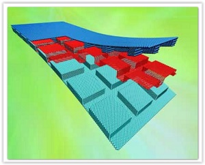
Rice simulations show that graphene between patterned gallium nitride and diamond would offer excellent heat transfer in next-generation hybrids of nano- and microelectronics.
Rice computer models replaced the flat interface between the materials with a nanostructured pattern and added a layer of graphene, the atom-thick form of carbon, as a way to dramatically improve heat transfer, said Rice materials scientist Rouzbeh Shahsavari.
The new work by Shahsavari, Rice graduate student and lead author Lei Tao and postdoctoral researcher Sreeprasad Sreenivasan appeared this month in the American Chemical Society journal ACS Applied Materials and Interfaces ("Interlaced, Nanostructured Interface with Graphene Buffer Layer Reduces Thermal Boundary Resistance in Nano/microelectronic Systems").
A patterned surface and a layer of atom-thick graphene helped transport phonons from the semiconductor to the heat sink
Rice University researchers used computer models to determine the best way to disperse heat produced by microelectronic devices using gallium nitride semiconductors and diamond. A patterned surface and a layer of atom-thick graphene helped transport phonons from the semiconductor to the heat sink. (Graphic by Lei Tao)
No matter the size, electronic devices need to disperse the heat they produce, Shahsavari said. “With the current trend of constant increases in power and device miniaturization, efficient heat management has become a serious issue for reliability and performance,” he said. “Oftentimes, the individual materials in hybrid nano- and microelectronic devices function well but the interface of different materials is the bottleneck for heat diffusion.”
Gallium nitride has become a strong candidate for use in high-power, high-temperature applications like uninterruptible power supplies, motors, solar converters and hybrid vehicles, he said. Diamond is an excellent heat sink, but its atomic interface with gallium nitride is hard for phonons to traverse.
The researchers simulated 48 distinct grid patterns with square or round graphene pillars and tuned them to match phonon vibration frequencies between the materials. Sinking a dense pattern of small squares into the diamond showed a dramatic decrease in thermal boundary resistance of up to 80 percent. A layer of graphene between the materials further reduced resistance by 33 percent.
Fine-tuning the pillar length, size, shape, hierarchy, density and order will be important, Lei said.
“With current and emerging advancements in nanofabrication like nanolithography, it is now possible to go beyond the conventional planer interfaces and create strategically patterned interfaces coated with nanomaterials to significantly boost heat transport,” Shahsavari said. “Our strategy is amenable to several other hybrid materials and provides novel insights to overcome the thermal boundary resistance bottleneck.”
Share on:


Suggested Items
SMC Korea 2024 to Highlight Semiconductor Materials Trends and Innovations on Industry’s Path to $1 Trillion
04/24/2024 | SEMIWith Korea a major consumer of semiconductor materials and advanced materials a key driver of innovation on the industry’s path to $1 trillion, industry leaders and experts will gather at SMC (Strategic Materials Conference) Korea 2024 on May 29 at the Suwon Convention Center in Gyeonggi-do, South Korea to provide insights into the latest materials developments and trends. Registration is open.
Groundbreaking Ceremony Marks the Beginning of a New Era for Newccess Industrial; The Construction of the MINGXIN Building
04/12/2024 | Newccess IndustrialOn a clear and sunny day in March, the groundbreaking ceremony for the MINGXIN Building took place in Shenzhen, China. This moment marked the official commencement of construction for a project that will reshape the semiconductor materials industry.
The Need for a Holistic Global Sustainability Standard
04/10/2024 | Michael Ford, Aegis SoftwareNo one can deny that the resources of our fragile planet are finite. The environment seems like a third party, subject to constant degradation. We’re acutely aware of the effects of pollution on our climate, and despite our “throw-away” culture, recycling and recovery of materials has remained relatively expensive, even as we use more energy just to survive.
iNEMI Publishes Four Roadmap Topics
04/04/2024 | iNEMIThe International Electronics Manufacturing Initiative (iNEMI) announces the availability of the first roadmap topics in the new iNEMI Roadmap format. Printed circuit boards, sustainable electronics, smart manufacturing, and mmWave materials and test are now available online.
Insulectro’s 'Storekeepers' Extend Their Welcome to Technology Village at IPC APEX EXPO
04/03/2024 | InsulectroInsulectro, the largest distributor of materials for use in the manufacture of PCBs and printed electronics, welcomes attendees to its TECHNOLOGY VILLAGE during this year’s IPC APEX EXPO at the Anaheim Convention Center, April 9-11, 2024.