


 Marcy's Musings: The Growing Industry
 It’s Only Common Sense: Here’s What To Do After IPC APEX EXPO 2024
 Dan’s Biz Bookshelf: Seeing the How
Perovskite Edges Can Be Tuned for Optoelectronic Performance
March 10, 2017 | Los Alamos National LaboratoryEstimated reading time: 2 minutes
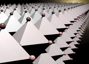
In the eternal search for next generation high-efficiency solar cells and LEDs, scientists at Los Alamos National Laboratory and their partners are creating innovative 2D layered hybrid perovskites that allow greater freedom in designing and fabricating efficient optoelectronic devices. Industrial and consumer applications could include low cost solar cells, LEDs, laser diodes, detectors, and other nano-optoelectronic devices.
“Our material is a layered compound, meaning it is a stack of 2D layers of perovskites with nanometer thickness (like a stack of sheets), and the 2D perovskite layers are separated by thin organic layers,” said Jean-Christophe Blancon, lead author on a paper out today in the journal Science’s First Release distribution. “This work could overturn conventional wisdom on the limitations of device designs based on layered perovskites.”
The 2D, near-single-crystalline “Ruddlesden-Popper” thin films have an out-of-plane orientation so that uninhibited charge transport occurs through the perovskite layers in planar devices. At the edges of the perovskite layers, the new research discovered “layer-edge-states,” which are key to both high efficiency of solar cells (>12 percent) and high fluorescence efficiency (a few tens of percent) for LEDs. The spontaneous conversion of excitons (bound electron-hole pairs) to free carriers via these layer-edge states appears to be the key to improving the photovoltaic and light-emitting thin-film layered materials.
The team investigated both photophysical and optoelectronic properties of phase-pure homogenous 2D perovskites. They were able to show that thin films have an intrinsic mechanism for dissociation of the strongly bound electron-hole pairs (excitons) to long-lived free-carriers provided by lower energy states at the edges of the layered perovskites.
Moreover, once carriers are trapped in these edge states, they remain protected and do not lose their energy via non-radiative processes. They can contribute to photocurrent in a photovoltaic (PV) device or radiatively recombine efficiently for light-emission applications. “These materials are quantum hybrid materials, possessing physical properties of both organic semiconductors and inorganic semiconducting quantum wells. We are just beginning to understand the interplay of the organic and inorganic components in 2D perovskites and this result underpins how unique properties can arise from competing physical properties,” said Jared Crochet of the Physical Chemistry and Applied Spectroscopy group at Los Alamos.
“These results address a long-standing problem not just for the perovskite family, but relevant to a large group of materials where edges and surface states generally degrade the optoelectronic properties, which can now be chemically designed and engineered to achieve efficient flow of charge and energy leading to high-efficiency optoelectronic devices,” said Aditya Mohite, who leads the perovskite program in the Material Synthesis and Integrated devices group at Los Alamos.
“The 2D hybrid perovskites continue to surprise. When we first designed these materials we were hoping that high quality samples of them would exhibit novel optoelectronic properties,” said co-author Mercouri Kanatzidis of Northwestern University. “Well, they have done so and then some. They have exceeded our expectations and are proving to be truly amazing systems. We have only scratched the surface of what is there—sorry for the pun—in this 2D family and we anticipate continued excitement going forward.”
Share on:


Suggested Items
Groundbreaking Ceremony Marks the Beginning of a New Era for Newccess Industrial; The Construction of the MINGXIN Building
04/12/2024 | Newccess IndustrialOn a clear and sunny day in March, the groundbreaking ceremony for the MINGXIN Building took place in Shenzhen, China. This moment marked the official commencement of construction for a project that will reshape the semiconductor materials industry.
The Need for a Holistic Global Sustainability Standard
04/10/2024 | Michael Ford, Aegis SoftwareNo one can deny that the resources of our fragile planet are finite. The environment seems like a third party, subject to constant degradation. We’re acutely aware of the effects of pollution on our climate, and despite our “throw-away” culture, recycling and recovery of materials has remained relatively expensive, even as we use more energy just to survive.
iNEMI Publishes Four Roadmap Topics
04/04/2024 | iNEMIThe International Electronics Manufacturing Initiative (iNEMI) announces the availability of the first roadmap topics in the new iNEMI Roadmap format. Printed circuit boards, sustainable electronics, smart manufacturing, and mmWave materials and test are now available online.
Insulectro’s 'Storekeepers' Extend Their Welcome to Technology Village at IPC APEX EXPO
04/03/2024 | InsulectroInsulectro, the largest distributor of materials for use in the manufacture of PCBs and printed electronics, welcomes attendees to its TECHNOLOGY VILLAGE during this year’s IPC APEX EXPO at the Anaheim Convention Center, April 9-11, 2024.
Checking In With ICAPE Group
04/03/2024 | Nolan Johnson, I-Connect007ICAPE Group’s field application engineer Erik Pederson drills down on sustainability, supply chain resiliency, and what value engineering really looks like in this exclusive interview. Founded in 1999, European-based ICAPE Group provides 21 million printed circuit boards and over six million technical parts to manufacturers every month. With 30 PCB manufacturing partners globally and 50 partners providing a wide array of technical parts, ICAPE Group has operations in China, Taiwan, Thailand, South Korea, Vietnam, South Africa, Europe, Mexico, and the United States. The company also focuses on the value proposition for its customers.