


 Marcy's Musings: The Growing Industry
 It’s Only Common Sense: Here’s What To Do After IPC APEX EXPO 2024
 Dan’s Biz Bookshelf: Seeing the How
Mapping the Effects of Crystal Defects
March 15, 2017 | MITEstimated reading time: 3 minutes
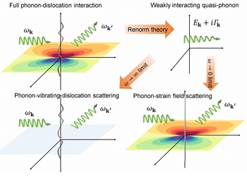
New research offers insights into how crystal dislocations — a common type of defect in materials — can affect electrical and heat transport through crystals, at a microscopic, quantum mechanical level.
Dislocations in crystals are places where the orderly three-dimensional structure of a crystal lattice — whose arrangement of atoms repeats with exactly the same spacing — is disrupted. The effect is as if a knife had sliced through the crystal and then the pieces were stuck back together, askew from their original positions. These defects have a strong effect on phonons, the modes of lattice vibration that play a role in the thermal and electrical properties of the crystals through which they travel. But a precise understanding of the mechanism of the dislocation-phonon interaction has been elusive and controversial, which has slowed progress toward using dislocations to tailor the thermal properties of materials.
A team at MIT has been able to learn important details about how those interactions work, which could inform future efforts to develop thermoelectric devices and other electronic systems. The findings are reported in the journal Nano Letters, in a paper co-authored by postdoc Mingda Li, Department of Mechanical Engineering head Professor Gang Chen, the late Institute Professor Emerita Mildred Dresselhaus, and five others.
Dislocations — which Li describes as “atomic irregularities in a regular crystal” — are very common defects in crystals, and they affect, for example, how heat dissipates through a silicon microchip or how well current flows through a silicon solar panel.
There have been two competing approaches to explaining phonon-dislocation interactions, Li explains, and a few other questions about them have remained unsolved. Now, the MIT team has found a new mathematical approach to analyzing such systems, using a new quasiparticle they formulated called a “dislon,” which is a quantized version of a dislocation, which seems to resolve these longstanding mysteries.
“People have tried to learn how the dislocations change the material properties — the electrical and thermal properties,” Li says. “Before now, there were many empirical models, which need fitting parameters to be complete. There was a long debate about the nature of phonon scattering in dislocations.”
The new theory, Li says, has a different starting point, as it is based on rigorous quantum field theory. It seems to resolve a number of issues, including a debate between two views known as the dynamic and static scattering approaches, showing they are simply
two extreme cases within this new framework. And while both of these approaches fail to explain behavior at the nanoscale, the new approach works well at such scales.
The findings could affect the search for better thermoelectric materials, which can convert heat to electricity. These are used for generating power from waste heat, or providing heaters for car seats. Thermoelectric systems can also provide cooling, for cold-drink chests, for example.
Chen, who is the Carl Richard Soderberg Professor of Power Engineering, attributes the new findings to Li’s initiative. “I didn’t put that much hope in it,” Chen said. “It’s a pretty complex problem: how dislocations affect these very important properties. ... I was very surprised when he came back with this new theory. He started from basic principles and derived a quantum description for it.”
Li and his team have made “a breakthrough by being able to account for the long-range nature of the dislocation strain field, by treating it as a new quantum mechanical object called the dislon,” says Jeffery Snyder, a professor at Northwestern University, who was not connected to this work. “Combining this with the quantum mechanical treatment of the dislon-electron interaction could lead to new strategies to optimize materials by using metallurgical approaches to engineer the structure, type, and location of dislocations within a material.”
“Dislocations have profound effects on properties of materials, but until now the long-range nature of the strain field has prevented direct calculations of dislocation effects,” says David J. Singh, a professor at the University of Missouri who also was not involved in this work. “The quantization developed in this paper goes a long way to solving these problems. I expect that this new formalism will lead to greatly improved understanding of the effects of dislocations on the electrical and thermal properties of materials. This work is a major step forward.”
The research team also included Zhiwei Ding, Jiawei Zhou, and Professor Hong Liu at MIT, and Qingping Meng and Yimei Zhu at Brookhaven National Laboratory. The work was supported by S3TEC, the Energy Frontier Research Center funded by the U.S. Department of Energy’s Office of Basic Energy Sciences, and the Defense Advanced Research Projects Agency of the U.S. Department of Defense.
Share on:


Suggested Items
Groundbreaking Ceremony Marks the Beginning of a New Era for Newccess Industrial; The Construction of the MINGXIN Building
04/12/2024 | Newccess IndustrialOn a clear and sunny day in March, the groundbreaking ceremony for the MINGXIN Building took place in Shenzhen, China. This moment marked the official commencement of construction for a project that will reshape the semiconductor materials industry.
The Need for a Holistic Global Sustainability Standard
04/10/2024 | Michael Ford, Aegis SoftwareNo one can deny that the resources of our fragile planet are finite. The environment seems like a third party, subject to constant degradation. We’re acutely aware of the effects of pollution on our climate, and despite our “throw-away” culture, recycling and recovery of materials has remained relatively expensive, even as we use more energy just to survive.
iNEMI Publishes Four Roadmap Topics
04/04/2024 | iNEMIThe International Electronics Manufacturing Initiative (iNEMI) announces the availability of the first roadmap topics in the new iNEMI Roadmap format. Printed circuit boards, sustainable electronics, smart manufacturing, and mmWave materials and test are now available online.
Insulectro’s 'Storekeepers' Extend Their Welcome to Technology Village at IPC APEX EXPO
04/03/2024 | InsulectroInsulectro, the largest distributor of materials for use in the manufacture of PCBs and printed electronics, welcomes attendees to its TECHNOLOGY VILLAGE during this year’s IPC APEX EXPO at the Anaheim Convention Center, April 9-11, 2024.
Checking In With ICAPE Group
04/03/2024 | Nolan Johnson, I-Connect007ICAPE Group’s field application engineer Erik Pederson drills down on sustainability, supply chain resiliency, and what value engineering really looks like in this exclusive interview. Founded in 1999, European-based ICAPE Group provides 21 million printed circuit boards and over six million technical parts to manufacturers every month. With 30 PCB manufacturing partners globally and 50 partners providing a wide array of technical parts, ICAPE Group has operations in China, Taiwan, Thailand, South Korea, Vietnam, South Africa, Europe, Mexico, and the United States. The company also focuses on the value proposition for its customers.