


 It’s Only Common Sense: OCCAM—the Time Is Now
 Marcy's Musings: The Growing Industry
 Dan’s Biz Bookshelf: Seeing the How
Researchers Uncover Secret of Nanomaterial That Makes Harvesting Sunlight Easier
March 29, 2017 | Imperial College LondonEstimated reading time: 2 minutes
Using sunlight to drive chemical reactions, such as artificial photosynthesis, could soon become much more efficient thanks to nanomaterials. Sunlight is used to drive many chemical processes that would not otherwise occur. For example, carbon dioxide and water do not ordinarily react, but in the process of photosynthesis, plants take these two chemicals and, using sunlight, produce oxygen and sugar.
The efficiency of this reaction is very high, meaning much of the energy from sunlight is transferred to the chemical reaction, but so far scientists have been unable to mimic this process in manmade artificial devices.
One reason is that many molecules that can undergo chemical reactions with light do not efficiently absorb the light themselves. They rely on photocatalysts – materials that absorb light efficiently and then pass the energy on to the molecules to drive reactions.
In the new study, researchers have investigated an artificial photocatalyst material using nanoparticles and found out how to make it more efficient.
This could lead to better solar panels, as the energy from the Sun could be more efficiently harvested. The photocatalyst could also be used to destroy liquid or gas pollutants, such as pesticides in water, by harnessing sunlight to drive reactions that break down the chemicals into less harmful forms.
Lead author Dr Emiliano Cortés from the Department of Physics at Imperial, said: “This finding opens new opportunities for increasing the efficiency of using and storing sunlight in various technologies.
“By using these materials we can revolutionize our current capabilities for storing and using sunlight with important implications in energy conversion, as well as new uses such as destroying pollutant molecules or gases and water cleaning, among others.”
Mighty nanomaterial
The material that the team investigated is made of metal nanoparticles – particles only billionths of a metre in diameter. Their results are published today in the Journal Nature Communications.
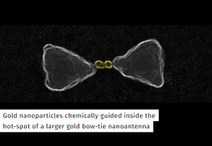
The team, which included researchers from the Chemistry Department at University of Duisburg-Essen in Germany led by Professor Sebastian Schlücker and theoreticians from the Rensselaer Polytechnic Institute and Harvard University at the US, showed that light-induced chemical reactions occur in certain regions over the surface of these nanomaterials.
They identified which areas of the nanomaterial would be most suitable for transferring energy to chemical reactions, by tracking the locations of very small gold nanoparticles (used as a markers) on the surface of the silver nanocatalytic material.
Now that they know which regions are responsible for the process of harvesting light and transferring it to chemical reactions, the team hope to be able to engineer the nanomaterial to increase these areas and make it more efficient.
Lead researcher Professor Stefan Maier said: “This is a powerful demonstration of how metallic nanostructures, which we have investigated in my group at Imperial for the last ten years, continue to surprise us in their abilities to control light on the nanoscale.
"The new finding uncovered by Dr Cortés and his collaborators in Germany and the US opens up new possibilities for this field in the areas photocatalysis and nanochemistry.”
Share on:


Suggested Items
KIC’s Miles Moreau to Present Profiling Basics and Best Practices at SMTA Wisconsin Chapter PCBA Profile Workshop
01/25/2024 | KICKIC, a renowned pioneer in thermal process and temperature measurement solutions for electronics manufacturing, announces that Miles Moreau, General Manager, will be a featured speaker at the SMTA Wisconsin Chapter In-Person PCBA Profile Workshop.
The Drive Toward UHDI and Substrates
09/20/2023 | I-Connect007 Editorial TeamPanasonic’s Darren Hitchcock spoke with the I-Connect007 Editorial Team on the complexities of moving toward ultra HDI manufacturing. As we learn in this conversation, the number of shifting constraints relative to traditional PCB fabrication is quite large and can sometimes conflict with each other.
Standard Of Excellence: The Products of the Future
09/19/2023 | Anaya Vardya -- Column: Standard of ExcellenceIn my last column, I discussed cutting-edge innovations in printed circuit board technology, focusing on innovative trends in ultra HDI, embedded passives and components, green PCBs, and advanced substrate materials. This month, I’m following up with the products these new PCB technologies are destined for. Why do we need all these new technologies?
Experience ViTrox's State-of-the-Art Offerings at SMTA Guadalajara 2023 Presented by Sales Channel Partner—SMTo Engineering
09/18/2023 | ViTroxViTrox, which aims to be the world’s most trusted technology company, is excited to announce that our trusted Sales Channel Partner (SCP) in Mexico, SMTo Engineering, S.A. de C.V., will be participating in SMTA Guadalajara Expo & Tech Forum. They will be exhibiting in Booth #911 from the 25th to the 26th of October 2023, at the Expo Guadalajara in Jalisco, Mexico.
Intel Unveils Industry-Leading Glass Substrates to Meet Demand for More Powerful Compute
09/18/2023 | IntelIntel announced one of the industry’s first glass substrates for next-generation advanced packaging, planned for the latter part of this decade.