


 Marcy's Musings: The Growing Industry
 It’s Only Common Sense: Here’s What To Do After IPC APEX EXPO 2024
 Dan’s Biz Bookshelf: Seeing the How
Researchers Create Artificial Materials Atom-By-Atom
March 29, 2017 | Aalto UniversityEstimated reading time: 3 minutes
Researchers at Aalto University have manufactured artificial materials with engineered electronic properties. By moving individual atoms under their microscope, the scientists were able to create atomic lattices with a predetermined electrical response. These results bring 'designer quantum materials' one step closer to reality.
The goal of nanoscience has always been to control matter at the smallest possible scale: The atoms which make up all objects around us. Atomic manipulation was achieved over two decades ago using a scanning tunnelling microscope (STM), and controlled positioning individual atoms and molecules has since become a favourite in the STM toolbox. But the possibility to precisely arrange the atoms on a sample brings new opportunities: By arranging atoms in a lattice, it becomes possible to engineer the electronic properties of the material through the atomic structure.
A collaboration of three research groups at Aalto University has now made this exciting prospect a reality. Combining ideas from experimental and theoretical physics, the groups headed by Professor Peter Liljeroth (Atomic Scale Physics), Academy Research Fellow Teemu Ojanen (Theory of Quantum Matter) and Senior University Lecturer Ari Harju (Quantum Many-Body Physics) demonstrated control over electronic properties in important model systems.
Working at a temperature of four degrees Kelvin, the researchers used state-of-the-art STM to arrange vacancies in a single layer of chlorine atoms supported on a copper crystal.
”The correspondence between atomic structure and electronic properties is of course what happens in real materials as well, but here we have complete control over the structure. In principle, we could target any electronic property and implement it experimentally”, says Dr. Robert Drost who carried out the experiments at Aalto University.
Using their atomic assembly method, the team demonstrated this by creating two real-life structures inspired by fundamental model systems with exotic electronic properties.
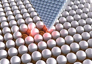
The tip of a scanning tunnelling microscope (STM) above chlorine atoms that have been deliberately moved. By moving individual atoms under their microscope, scientists were able to arrange vacancies in a single layer of chlorine atoms and create atomic lattices with a predetermined electrical response. Photo Ella Maru Studio.
The approach is not limited to the chlorine system chosen by the research team either. The same method can be applied in many well-understood systems in surface and nanoscience and could even be adapted to mesoscopic systems, such as quantum dots, which are controlled through lithographic processes.
”The approach is extremely versatile. In principle, we could target any electronic property we might want. Many things which can be shown to be possible in theory, we could probably implement”, continues Drost.
The systems studied by the researchers were inspired by theoretical models of fundamental importance. The first system, a so-called dimer chain, can have topological domain wall states, and the researchers were able to create these in the desired atomic positions by controlling the structure.
“The study of topological quantum materials is one of the most active research topics in contemporary physics. Our results establish that the field has matured to the point where exotic phases of matter can be designed and artificially fabricated”, explains Teemu Ojanen.
The other system investigated, the Lieb lattice, has exotic electronic structure that might be of relevance for realizing artificial magnetic or superconducting systems.
“This system is predicted to have a so-called flat band, where electrons behave as if they had infinite mass and this could result in magnetism or superconductivity. We will test this in future research”, explains Ari Harju.
"Our results open up a new area of research where the close collaboration of experimental and theoretical groups will certainly lead to many exciting discoveries. We are setting up a new centre of excellence on Designer Matter for achieving exactly this. It is rare that we can dream up some structure with exciting properties and then directly walk to the lab and actually realize it in practise”, concludes Liljeroth.
Share on:


Suggested Items
Insulectro’s 'Storekeepers' Extend Their Welcome to Technology Village at IPC APEX EXPO
04/03/2024 | InsulectroInsulectro, the largest distributor of materials for use in the manufacture of PCBs and printed electronics, welcomes attendees to its TECHNOLOGY VILLAGE during this year’s IPC APEX EXPO at the Anaheim Convention Center, April 9-11, 2024.
ENNOVI Introduces a New Flexible Circuit Production Process for Low Voltage Connectivity in EV Battery Cell Contacting Systems
04/03/2024 | PRNewswireENNOVI, a mobility electrification solutions partner, introduces a more advanced and sustainable way of producing flexible circuits for low voltage signals in electric vehicle (EV) battery cell contacting systems.
Heavy Copper PCBs: Bridging the Gap Between Design and Fabrication, Part 1
04/01/2024 | Yash Sutariya, Saturn Electronics ServicesThey call me Sparky. This is due to my talent for getting shocked by a variety of voltages and because I cannot seem to keep my hands out of power control cabinets. While I do not have the time to throw the knife switch to the off position, that doesn’t stop me from sticking screwdrivers into the fuse boxes. In all honesty, I’m lucky to be alive. Fortunately, I also have a talent for building high-voltage heavy copper circuit boards. Since this is where I spend most of my time, I can guide you through some potential design for manufacturability (DFM) hazards you may encounter with heavy copper design.
Trouble in Your Tank: Supporting IC Substrates and Advanced Packaging, Part 5
03/19/2024 | Michael Carano -- Column: Trouble in Your TankDirect metallization systems based on conductive graphite or carbon dispersion are quickly gaining acceptance worldwide. Indeed, the environmental and productivity gains one can achieve with these processes are outstanding. In today’s highly competitive and litigious environment, direct metallization reduces costs associated with compliance, waste treatment, and legal issues related to chemical exposure. What makes these processes leaders in the direct metallization space?
AT&S Shines with Purest Copper on World Recycling Day
03/18/2024 | AT&SThe Styrian microelectronics specialist AT&S is taking World Recycling Day as an opportunity to review the progress that has been made in recent months at its sites around the world in terms of the efficient use of resources: