


 It’s Only Common Sense: OCCAM—the Time Is Now
 Marcy's Musings: The Growing Industry
 Dan’s Biz Bookshelf: Seeing the How
Collaborative Materials Research Creates Potential for Improved Computer Chips and Transistors
May 15, 2017 | Texas A&M UniversityEstimated reading time: 4 minutes
It’s a material world, and an extremely versatile one at that, considering its most basic building blocks — atoms — can be connected together to form different structures that retain the same composition.
Diamond and graphite, for example, are but two of the many polymorphs of carbon, meaning that both have the same chemical composition and differ only in the manner in which their atoms are connected. But what a world of difference that connectivity makes: the former goes into a ring and costs thousands of dollars, while the latter has to sit content within a humble pencil.
The inorganic compound hafnium dioxide commonly used in optical coatings likewise has several polymorphs, including a tetragonal form with highly attractive properties for computer chips and other optical elements. However, because this form is stable only at temperatures above 3100 degrees Fahrenheit — think blazing inferno — scientists have had to make do with its more limited monoclinic polymorph, until now.
A team of researchers led by University of Kentucky chemist Beth Guiton and Texas A&M University chemist Sarbajit Banerjee in collaboration with Texas A&M materials science engineer Raymundo Arróyave and University of Buffalo chemist Sean Depner, has found a way to achieve this highly sought tetragonal phase at 1100 degrees Fahrenheit — think much closer to room temperature and potential holy grail for the computing industry, along with countless other sectors and applications.
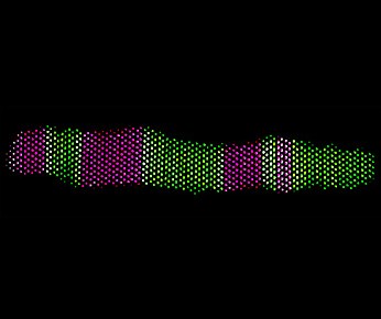
The team’s research, published this week in Nature Communications, details their observation of this spectacular atom-by-atom transformation, witnessed with the help of incredibly powerful microscopes at Oak Ridge National Laboratory as they heated tiny crystal nanorods composed of shrunken monoclinic hafnium dioxide particles. Each nanorod featured a barcode-like structure, complete with twin nanoscale, fault-forming stripes that serve as ground zero for the transition.
Banerjee Lab“In this study we are watching a tiny metal oxide rod transform from one structure, which is the typical material found at room temperature, into a different, related structure not usually stable below 3100 degrees Fahrenheit,” Guiton said. “This is significant because the high-temperature material has amazing properties that make it a candidate to replace silicon dioxide in the semiconductor industry, which is built on silicon.”
The semiconductor industry has long relied on silicon dioxide as its thin, non-conductive layer of choice in the critical gap between the gate electrode — the valve that turns a transistor on and off — and the silicon transistor. Consistently thinning this non-conductive layer is what allows transistors to become smaller and faster, but Guiton points out there is such a thing as too thin — the point at which electrons start sloshing across the barrier, thereby heating their surroundings and draining power. She says most of us have seen and felt this scenario to some degree (pun intended), for instance, while watching videos on our phones and the battery simultaneously drain as the device in our palm noticeably begins to warm.
As computer chips become smaller, faster and more powerful, their insulating layers must also be much more robust — currently a limiting factor for semiconductor technology. Guiton says this new phase of hafnia is an order of magnitude better at withstanding applied fields.
When it comes to watching hafnia’s structural transition between its traditional monoclinic state and this highly sought-after tetragonal phase at much closer to room temperature, Banerjee says it’s not unlike popular television — specifically, the “Hall of Faces” in the HBO show “Game of Thrones.”
“In essence, we have been able to watch in real time, on an atom by atom basis, as hafnia is transformed to a new phase, much like Arya Stark donning a new face,” Banerjee said. “The new phase of hafnia has a much higher ‘k’ value representing its ability to store charge, which would allow transistors to work really quickly while merely sipping on power instead of sapping it. The stripes turn out to be really important, since that is where the transition starts as the hafnia loses its stripes."
Raymundo ArroyaveArróyave credits real-time atomic-scale information for enabling the group to figure out that the transformation occurs in a very different way at nanoscale levels than it does within the macroscopic particles that result in hafnia's monoclinic form. The fact that it is nanoscale in the first place is why he says the transition occurs at, or much closer to, room temperature.
“Through synthesis at the nanoscale, the ‘height’ of the energy barrier separating the two forms has been shrunk, making it possible to observe tetragonal hafnia at much lower temperatures than usual,” Arróyave said. “This points toward strategies that could be used to stabilize a host of useful forms of materials that can enable a wide range of functionalities and associated technologies. This is just one example of the vast possibilities that exist when we start to explore the ‘metastable’ materials space.”
Banerjee says this study suggests one way to stabilize the tetragonal phase at actual room temperature — which he notes that his group previously accomplished via a different method last year — and big implications for fast low-power-consumption transistors capable of controlling currents without drawing power, reducing speed or producing heat.
“The possibilities are endless, including even more powerful laptops that don’t heat up and sip on power from their batteries and smart phones that ‘keep calm and carry on,’” Banerjee said. “We are trying to apply these same tricks to other polymorphs of hafnium dioxide and other materials — isolating other phases that are not readily stabilized at room temperature but may also have strange and desirable properties.”
The team’s research was supported in part by the U.S. Department of Energy, NASA Kentucky, the National Science Foundation and the Air Force Office of Scientific Research.
This article was written by Shana K. Hutchins, Texas A&M University College of Science and originally appeared on the College of Science website.
Share on:


Suggested Items
New Book on Low-temperature Soldering Now Available
04/17/2024 | I-Connect007I-Connect007 is pleased to announce that The Printed Circuit Assembler’s Guide to… Low-temperature Soldering, Vol. 2, by subject matter experts at MacDermid Alpha Electronics Solutions, is now available for download.
The Chemical Connection: Reducing Etch System Water Usage, Part 1
04/05/2024 | Don Ball -- Column: The Chemical ConnectionWater conservation has become an important component of the overall system design for most manufacturing operations today. Changing climate conditions and increasing populations are beginning to strain the freshwater supplies in many areas of the country. As a result, as equipment suppliers, we see an increasing number of requests for options that reduce water usage in proposed wet processing systems. Etching systems tend to use more water because of the need for close temperature control to maintain steady etch rates and the rinsing requirements for complete removal of corrosive etchants from the surface of the product before the next process step. This column contains some simple suggestions for reducing water usage in etch systems that won’t strain the budget too much.
Indium’s Sze Pei Lim to Present on Semiconductor Packaging at ICEP Japan
04/02/2024 | Indium CorporationIndium Corporation’s Senior Global Product Manager for Semiconductor and Advanced Materials, Sze Pei Lim, is scheduled to present at the International Conference on Electronics Packaging (ICEP 2024).
Nihon Superior Sets New Standards in Lead-Free Soldering Technology at APEX 2024
03/13/2024 | PVANihon Superior Co. Ltd., an advanced joining material supplier, will exhibit in Booth 1325 during the 2024 IPC APEX EXPO, scheduled to take place April 9-11, 2024 at the Anaheim Convention Center in California.
Indium Corporation to Showcase Proven EV Products and High-Reliability Alloys at Productronica China
02/28/2024 | Indium CorporationAs a materials pioneer and trusted partner in electric vehicle (EV) and e-Mobility manufacturing, Indium Corporation is proud to showcase its high-reliability alloys and soldering solutions at Productronica China, March 20-22, in Shanghai.