


 It’s Only Common Sense: OCCAM—the Time Is Now
 Marcy's Musings: The Growing Industry
 Dan’s Biz Bookshelf: Seeing the How
Micro LED-Like Products Breakthrough in Mass Transfer Have yet to Materialize
July 20, 2017 | TrendForceEstimated reading time: 3 minutes
A major bottleneck in the commercialization of Micro LED displays is the mass transfer of micron-size LEDs to a display backplane. Research by LEDinside, a division of TrendForce, reveals that many companies across industries worldwide have entered the Micro LED market and are in a race to develop methods for the mass transfer process. However, their solutions have yet to meet the standard for commercialization in terms of production output (in unit per hour, UPH), transfer yield and size of LED chips (i.e. Micro LED is technically defined as LEDs that are smaller than 100 microns). These research findings can be found in LEDinside’s 3Q17 Micro LED Next Generation Display Industry Member Report: Analyses on Mass Transfer and Inspection/Repair Technologies.
Currently, entrants in the Micro LED market are working towards the mass transfer of LEDs sized around 150 microns. LEDinside anticipates that displays and projection modules featuring 150-micron LEDs will be available on the market as early as 2018. When the mass transfer for LEDs of this size matures, market entrants will then invest in processes for making smaller products.
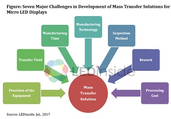
Development of mass transfer solutions faces seven major challenges
“Mass transfer is one of the four main stages in the manufacturing of Micro LED displays and has many highly difficult technological challenges,” said Simon Yang, assistant research manager of LEDinside. Yang pointed out that developing a cost-effective mass transfer solution depends on advances in seven key areas: precision of the equipment, transfer yield, manufacturing time, manufacturing technology, inspection method, rework and processing cost.
LED suppliers, semiconductor makers and companies across the display supply chain will have to work together to develop specification standards for materials, chips and fabrication equipment used in Micro LED production. Cross-industry collaboration is necessary since each industry has its own specification standards. Also, an extended period of R&D is needed to overcome the technological hurdles and integrate various fields of manufacturing.
Mass transfer has to achieve five-sigma level before mass production of Micro LED displays is feasible
Using Six Sigma as the model for determining the feasibility of mass production of Micro LED displays, LEDinside’s analysis indicates that the yield of the mass transfer process must reach the four-sigma level to make commercialization possible. However, the processing cost and the costs related to inspection and defect repair are still quite high even at the four-sigma level. To have commercially mature products with competitive processing cost available for market release, the mass transfer process has to reach the five-sigma level or above in transfer yield.
As progress on mass transfer solutions continues, true Micro LED products are expected to first enter applications such as indoor displays and wearables
Even though no major breakthroughs have been announced, many technology companies and research agencies worldwide continue to invest in the R&D of mass transfer process. Some of the well-known international enterprises and institutions working in this area are LuxVue, eLux, VueReal, X-Celeprint, CEA-Leti, SONY and OKI. Comparable Taiwan-based companies and organizations include PlayNitride, Industrial Technology Research Institute, Mikro Mesa and TSMC.
There are several types of mass transfer solutions under development. Choosing one of them will depend on various factors such as application markets, equipment capital, UPH and processing cost. Additionally, the expansion of manufacturing capacity and the raising of the yield rate are important to product development.
According to the latest developments, LEDinside believes that the markets for wearables (e.g. smartwatches and smart bracelets) and large indoor displays will first see Micro LED products (LEDs sized under 100 microns). Because mass transfer is technologically challenging, market entrants will initially use the existing wafer bonding equipment to build their solutions. Furthermore, each display application has its own pixel volume specifications, so market entrants will likely focus on products with low pixel volume requirements as to shorten the product development cycle.
Thin film transfer is another away of moving and arranging micron-size LEDs, and some market entrants are making a direct jump to developing solutions under this approach. However, perfecting thin film transfer will take longer time and more resources because equipment for this method will have to be designed, built and calibrated. Such an undertaking will also involve difficult manufacturing related issues.
Share on:


Suggested Items
IDTechEx Report Unveils 3D Electronics Status and Opportunities
04/22/2024 | PRNewswire3D electronics is an emerging manufacturing approach that enables electronics to be integrated within or onto the surface of objects. 3D electronic manufacturing techniques empower new features, including mass customizability, greater integration, and improved sustainability in the electronics industry.
IDTechEx Examines the Opportunities for Wearables in Digital Health
04/19/2024 | IDTechExIDTechEx’s report, “Digital Health and Artificial Intelligence 2024-2034: Trends, Opportunities, and Outlook”, covers this ongoing trend in the consumer health wearables market and includes analysis of the opportunities and roadmap for biometric monitoring.
Real Time with... IPC APEX EXPO 2024: Pluritec's Expansion and Growth in the North American Market
04/19/2024 | Real Time with...IPC APEX EXPONicola Doria, president of Pluritec, discusses the company's strategic focus on the North American market, their investment in a new sales organization, service expansion, and a new process integration line. The conversation also covers market response and future installations, as well as Pluritec's new partnership with IEC.
Mycronic Releases Interim Report January–March 2024
04/18/2024 | MycronicNet sales increased 39 percent to SEK 1,692 (1,219) million. Based on constant exchange rates, net sales increased 42 percent.
Real Time with... IPC APEX EXPO 2024: Exploring Silicone Solutions with R&D Director of CHT
04/17/2024 | Real Time with...IPC APEX EXPOIn this interview, Gerry Ellis, the R&D director for CHT, discusses the product range offered by his company. He explains the challenges in creating base formulations, the drive to make products more user-friendly, and the various application techniques involved. Ellis also highlights the key market segments and the significance of providing efficient solutions to customers.