


 It’s Only Common Sense: OCCAM—the Time Is Now
 Marcy's Musings: The Growing Industry
 Dan’s Biz Bookshelf: Seeing the How
Biodegradable Electronics
October 13, 2017 | Fraunhofer FEPEstimated reading time: 1 minute
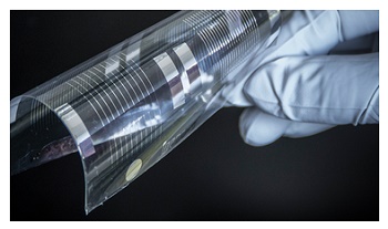
Under the direction of the Fraunhofer Institute for Organic Electronics, Electron Beam and Plasma Technology FEP, an in-house Fraunhofer project for development of biodegradable electronics was begun last year. The Fraunhofer Institute for Electronic Nano Systems ENAS, the Fraunhofer Institute for Biomedical Engineering IBMT, the Fraunhofer Institute for Silicate Research ISC, and the Fraunhofer Resource Recycling and Strategy Project Group IWKS are working together on the project.
Electronic components that are completely broken down in a biological environment after a pre-defined operating life open up novel applications as well as ways for reducing their ecological footprint.
One enabling technology for such components is the manufacture of biodegradable conductive traces on biodegradable substrates using vacuum technologies. This technology was developed by Fraunhofer FEP.
A novel application area for these innovative electronic components for example is in the field of active medical implants that after expiration of their operating life are resorbed by tissue, thereby sparing the patient a second surgical intervention.
The Fraunhofer Gesellschaft e. V. is now funding the "bioElektron - Biodegradable Electronics for Active Implants" project through its in-house program (funding No. MAVO B31 301). The goal of the project is the development of essential components for biodegradable electronic parts that can be employed for example in an implant.
This includes in particular:
- biodegradable conductor structures
- biodegradable electrodes for collecting electrical signals or delivering electrical stimulation
- biodegradable thin-film transistors and circuitry
- biodegradable barrier coatings as moisture and gas barriers, and electrical insulation layers
These elements will be monolithically integrated into a flexible thin-film device.
Conductor structures and organic thin-film transistors are being developed at Fraunhofer FEP using vacuum technology. Deposition of magnesium via thermal evaporation under high vacuum conditions is being used as an enabling technology for this purpose. Magnesium is known for being a biodegradable and biologically compatible metal that is already employed in clinical environments as an absorbable implant material. The challenge consists of depositing this metal upon biodegradable polymer films that magnesium does not adhere sufficiently to under normal process control. By suitably pre-treating the substrates using a combination of drying, plasma treatment, and utilization of seed layers, finely structured high-quality conductor structures were able to be produced.
Share on:


Suggested Items
SMC Korea 2024 to Highlight Semiconductor Materials Trends and Innovations on Industry’s Path to $1 Trillion
04/24/2024 | SEMIWith Korea a major consumer of semiconductor materials and advanced materials a key driver of innovation on the industry’s path to $1 trillion, industry leaders and experts will gather at SMC (Strategic Materials Conference) Korea 2024 on May 29 at the Suwon Convention Center in Gyeonggi-do, South Korea to provide insights into the latest materials developments and trends. Registration is open.
Orbex Secures £16.7m Investment for Rocket ‘Ramp Up’ Period
04/24/2024 | OrbexThe UK spaceflight company Orbex has received £16.7m from six backers in an update to its Series C funding round.
Real Time with... IPC APEX EXPO 2024: Going Vertical: SCHMID's Advanced Solutions for Printed Circuit Boards
04/24/2024 | Real Time with...IPC APEX EXPOEditor Marcy LaRont chats with Bob Ferguson, the president of SCHMID, about advanced solutions for PCBs and the equipment they are highlighting at this year's show. He delves into vertical no-touch handling systems and the prospect of achieving sub-10-micron lines. Inspired by SCHMID's technology, Bob expresses excitement about where the industry is today.
Real Time with... IPC APEX EXPO 2024: Advancements in Laser Depaneling with LPKF
04/24/2024 | Real Time with...IPC APEX EXPOJake Benz, LPKF sales manager for North America, discusses the company's advancements in laser depaneling. LPKF has introduced a green wavelength laser for processing rigid FR-4 circuit boards, bringing significant gains in processing speeds to market. The company transitioned from IR CO2 to UV wavelength due to heat and burning issues.
Adura Solutions Exhibits at Del Mar 2024
04/24/2024 | Adura SolutionsSumit Tomar, CEO of Adura Solutions, has announced that his company will be exhibiting at this year’s Del Mar Electronics and Manufacturing Show to be held at the Del Mar Fairgrounds, San Diego, California, April 24-25.