


 Marcy's Musings: The Growing Industry
 It’s Only Common Sense: Here’s What To Do After IPC APEX EXPO 2024
 Dan’s Biz Bookshelf: Seeing the How
Think Laterally to Sidestep Production Problems
October 16, 2017 | KAUSTEstimated reading time: 2 minutes
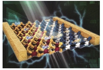
Super thin photovoltaic devices underpin solar technology and gains in the efficiency of their production are therefore keenly sought. KAUST researchers have combined and rearranged different semiconductors to create so-called lateral p-n heterojunctions—a simpler process they hope will transform the fabrication of solar cells, self-powered nanoelectronics as well as ultrathin, transparent, flexible devices.
Two-dimensional semiconductor monolayers, such as graphene and transition-metal dichalcogenides like WSe2 and MoS2, have unique electrical and optical properties that make them potential alternatives to conventional silicon-based materials. Recent advances in material growth and transfer techniques have allowed scientists to manipulate these monolayers. Specifically, vertical stacking has led to ultrathin photovoltaic devices but requires multiple complex transfer steps. These steps are hampered by various issues, such as the formation of contaminants and defects at the monolayer interface, which limit device quality.
“Devices obtained using these transfer techniques are usually unstable and vary from sample to sample,” says lead researcher and former visiting student of Associate Professor, Jr-Hau He, Meng-Lin Tsai, who adds that transfer-related contaminants significantly affect device reliability. Electronic properties have also proven difficult to control by vertical stacking.
To fully harness the exceptional properties of these two-dimensional materials, Tsai’s team, under the mentorship of He, created monolayers featuring lateral WSe2–MoS2 heterojunctions and incorporated them into solar cells. Under simulated sunlight, the cells achieved greater power conversion efficiency than their vertically stacked equivalents.
To do this, first the researchers synthesized the heterojunctions by consecutively depositing WSe2 and MoS2 on a sapphire substrate. Next, they transferred the materials onto a silicon-based surface for photovoltaic device fabrication.
High-resolution microscopy revealed that the lateral junction displayed a clear separation between the semiconductors at the interface. Also, the researchers detected no discernable height difference between semiconductor regions, consistent with an atomically thin interface.
These interfacial characteristics signaled success. “Our structures are cleaner and more ideal than vertically stacked assemblies because we didn’t need the multi-step transfer procedure,” explains Tsai.
Furthermore, the lateral heterojunctions mostly retained their efficiency despite changes to the orientation of the incident light. Being able to take light coming from any direction means expensive solar tracking systems will become redundant.
According to Tsai, the implementation of lateral heterojunctions in more complex circuits and interconnects may result in higher performance than in conventional solar cells and so the team is working on the next steps. “We are trying to understand the underlying kinetics and thermodynamics of these heterojunctions to design more efficient cells," he adds.
Share on:


Suggested Items
Groundbreaking Ceremony Marks the Beginning of a New Era for Newccess Industrial; The Construction of the MINGXIN Building
04/12/2024 | Newccess IndustrialOn a clear and sunny day in March, the groundbreaking ceremony for the MINGXIN Building took place in Shenzhen, China. This moment marked the official commencement of construction for a project that will reshape the semiconductor materials industry.
The Need for a Holistic Global Sustainability Standard
04/10/2024 | Michael Ford, Aegis SoftwareNo one can deny that the resources of our fragile planet are finite. The environment seems like a third party, subject to constant degradation. We’re acutely aware of the effects of pollution on our climate, and despite our “throw-away” culture, recycling and recovery of materials has remained relatively expensive, even as we use more energy just to survive.
iNEMI Publishes Four Roadmap Topics
04/04/2024 | iNEMIThe International Electronics Manufacturing Initiative (iNEMI) announces the availability of the first roadmap topics in the new iNEMI Roadmap format. Printed circuit boards, sustainable electronics, smart manufacturing, and mmWave materials and test are now available online.
Insulectro’s 'Storekeepers' Extend Their Welcome to Technology Village at IPC APEX EXPO
04/03/2024 | InsulectroInsulectro, the largest distributor of materials for use in the manufacture of PCBs and printed electronics, welcomes attendees to its TECHNOLOGY VILLAGE during this year’s IPC APEX EXPO at the Anaheim Convention Center, April 9-11, 2024.
Checking In With ICAPE Group
04/03/2024 | Nolan Johnson, I-Connect007ICAPE Group’s field application engineer Erik Pederson drills down on sustainability, supply chain resiliency, and what value engineering really looks like in this exclusive interview. Founded in 1999, European-based ICAPE Group provides 21 million printed circuit boards and over six million technical parts to manufacturers every month. With 30 PCB manufacturing partners globally and 50 partners providing a wide array of technical parts, ICAPE Group has operations in China, Taiwan, Thailand, South Korea, Vietnam, South Africa, Europe, Mexico, and the United States. The company also focuses on the value proposition for its customers.