


 Marcy's Musings: The Growing Industry
 It’s Only Common Sense: Here’s What To Do After IPC APEX EXPO 2024
 Dan’s Biz Bookshelf: Seeing the How
Researchers Develop Flexible, Stretchable Photonic Devices
November 8, 2017 | MITEstimated reading time: 4 minutes
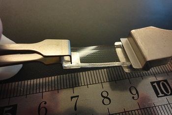
Researchers at MIT and several other institutions have developed a method for making photonic devices — similar to electronic devices but based on light rather than electricity — that can bend and stretch without damage. The devices could find uses in cables to connect computing devices, or in diagnostic and monitoring systems that could be attached to the skin or implanted in the body, flexing easily with the natural tissue.
The findings, which involve the use of a specialized kind of glass called chalcogenide, are described in two papers by MIT Associate Professor Juejun Hu and more than a dozen others at MIT, the University of Central Florida, and universities in China and France. The paper is slated for publication soon in Light: Science and Applications.
Hu, who is the Merton C. Flemings Associate Professor of Materials Science and Engineering, says that many people are interested in the possibility of optical technologies that can stretch and bend, especially for applications such as skin-mounted monitoring devices that could directly sense optical signals. Such devices might, for example, simultaneously detect heart rate, blood oxygen levels, and even blood pressure.
Photonics devices process light beams directly, using systems of LEDs, lenses, and mirrors fabricated with the same kinds of processes used to manufacture electronic microchips. Using light beams rather than a flow of electrons can have advantages for many applications; if the original data is light-based, for example, optical processing avoids the need for a conversion process.
But most current photonics devices are fabricated from rigid materials on rigid substrates, Hu says, and thus have an “inherent mismatch” for applications that “should be soft like human skin.” But most soft materials, including most polymers, have a low refractive index, which leads to a poor ability to confine a light beam.
Instead of using such flexible materials, Hu and his team took a novel approach: They formed the stiff material — in this case a thin layer of a type of glass called chalcogenide — into a spring-like coil. Just as steel can be made to stretch and bend when formed into a spring, the architecture of this glass coil allows it to stretch and bend freely while maintaining its desirable optical properties.
“You end up with something as flexible as rubber, that can bend and stretch, and still has a high refractive index and is very transparent,” Hu says. Tests have shown that such spring-like configurations, made directly on a polymer substrate, can undergo thousands of stretching cycles with no detectable degradation in their optical performance. The team produced a variety of photonic components, interconnected by the flexible, spring-like waveguides, all in an epoxy resin matrix, which was made stiffer near the optical components and more flexible around the waveguides.
Other kinds of stretchable photonics have been made by embedding nanorods of a stiffer material in a polymer base, but those require extra manufacturing steps and are not compatible with existing photonic systems, Hu says.
Such flexible, stretchable photonic circuits could also be useful for applications where the devices need to conform to the uneven surfaces of some other material, such as in strain gauges. Optics technology is very sensitive to strain, according to Hu, and could detect deformations of less than one-hundredth of 1 percent.
This research is still in early stages; Hu’s team has demonstrated only single devices at a time thus far. “For it to be useful, we have to demonstrate all the components integrated on a single device,” he says. Work is ongoing to develop the technology to that point so that it could be commercially applied, which Hu says could take another two to three years.
In another paper published last week in Nature Photonics, Hu and his collaborators have also developed a new way of integrating layers of photonics, made of chalcogenide glass and two-dimensional materials such as graphene, with conventional semiconductor photonic circuitry. Existing methods for integrating such materials require them to be made on one surface and then peeled off and transferred to the semiconductor wafer, which adds significant complexity to the process. Instead, the new process allows the layers to be fabricated directly on the semiconductor surface, at room temperature, allowing for simplified fabrication and more precise alignment.
The process can also make use of the chalcogenide material as a “passivation layer,” to protect 2-D materials from degradation caused by ambient moisture, and as a way to control the optoelectronic characteristics of 2-D materials. The method is generic and could be extended to other emerging 2-D materials besides graphene, to expand and expedite their integration with photonic circuitry, Hu says.
The research team also included MIT Professor Jing Kong, MIT postdocs Lan Li and Hongtao Lin, and others at the University of Texas, Xiamen University and Chongqing University in China, Universite Paris-Sud in France, the University of Southampton in the UK, and the University of Central Florida. The work was supported by the National Science Foundation and made use of the MIT Microsystems Technology Laboratories.
Share on:


Suggested Items
Groundbreaking Ceremony Marks the Beginning of a New Era for Newccess Industrial; The Construction of the MINGXIN Building
04/12/2024 | Newccess IndustrialOn a clear and sunny day in March, the groundbreaking ceremony for the MINGXIN Building took place in Shenzhen, China. This moment marked the official commencement of construction for a project that will reshape the semiconductor materials industry.
The Need for a Holistic Global Sustainability Standard
04/10/2024 | Michael Ford, Aegis SoftwareNo one can deny that the resources of our fragile planet are finite. The environment seems like a third party, subject to constant degradation. We’re acutely aware of the effects of pollution on our climate, and despite our “throw-away” culture, recycling and recovery of materials has remained relatively expensive, even as we use more energy just to survive.
iNEMI Publishes Four Roadmap Topics
04/04/2024 | iNEMIThe International Electronics Manufacturing Initiative (iNEMI) announces the availability of the first roadmap topics in the new iNEMI Roadmap format. Printed circuit boards, sustainable electronics, smart manufacturing, and mmWave materials and test are now available online.
Insulectro’s 'Storekeepers' Extend Their Welcome to Technology Village at IPC APEX EXPO
04/03/2024 | InsulectroInsulectro, the largest distributor of materials for use in the manufacture of PCBs and printed electronics, welcomes attendees to its TECHNOLOGY VILLAGE during this year’s IPC APEX EXPO at the Anaheim Convention Center, April 9-11, 2024.
Checking In With ICAPE Group
04/03/2024 | Nolan Johnson, I-Connect007ICAPE Group’s field application engineer Erik Pederson drills down on sustainability, supply chain resiliency, and what value engineering really looks like in this exclusive interview. Founded in 1999, European-based ICAPE Group provides 21 million printed circuit boards and over six million technical parts to manufacturers every month. With 30 PCB manufacturing partners globally and 50 partners providing a wide array of technical parts, ICAPE Group has operations in China, Taiwan, Thailand, South Korea, Vietnam, South Africa, Europe, Mexico, and the United States. The company also focuses on the value proposition for its customers.