


 It’s Only Common Sense: OCCAM—the Time Is Now
 Marcy's Musings: The Growing Industry
 Dan’s Biz Bookshelf: Seeing the How
Researchers Discover Method to 3D Print Fully Functional Circuits
November 10, 2017 | University of NottinghamEstimated reading time: 3 minutes
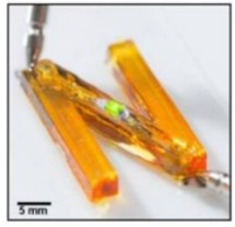
Researchers at the University of Nottingham have pioneered a breakthrough method to rapidly 3D print fully functional electronic circuits.
The circuits, which contain electrically-conductive metallic inks and insulating polymeric inks, can now be produced in a single inkjet printing process where a UV light rapidly solidifies the inks.
The breakthrough technique paves the way for the electronics manufacturing industry to produce fully functional components such as 3D antennae and fully printed sensors from multiple materials including metals and plastics.
The new method combines 2D printed electronics with Additive Manufacturing (AM) or 3D printing -- which is based on layer-by-layer deposition of materials to create 3D products. This expands the impact of Multifunctional Additive Manufacturing (MFAM), which involves printing multiple materials in a single additive manufacturing system to create components that have broader functionalities.
The new method overcomes some of the challenges in manufacturing fully functional devices that contain plastic and metal components in complex structures, where different methods are required to solidify each material.
Existing systems typically use just one material which limits the functionality of the printed structures. Having two materials like a conductor and an insulator, expands the range of functions in electronics. For example, a wristband which includes a pressure sensor and wireless communication circuitry could be 3D printed and customised for the wearer in a single process.
The breakthrough speeds up the solidification process of the conductive inks to less than a minute per layer. Previously, this process took much longer to be completed using conventional heat sources such as ovens and hot plates, making it impractical when hundreds of layers are needed to form an object. In addition, the production of electronic circuits and devices is limited by current manufacturing methods that restrict both the form and potentially the performance of these systems.
Professor Chris Tuck, Professor of Materials Engineering and lead investigator of the study, highlighted the potential of the breakthrough, 'Being able to 3D print conductive and dielectric materials (electrical insulators) in a single structure with the high precision that inkjet printing offers, will enable the fabrication of fully customised electronic components. You don't have to select standard values for capacitors when you design a circuit, you just set the value and the printer will produce the component for you.'
Professor Richard Hague, Director of the Centre for Additive Manufacturing (CfAM) added, 'Printing fully functional devices that contain multiple materials in complex, 3D structures is now a reality. This breakthrough has significant potential to be the enabling manufacturing technique for 21st century products and devices that will have the potential to create a significant impact on both the industry and the public.'
How it works
Dr. Ehab Saleh and members of the team from CfAM found that silver nanoparticles in conductive inks are capable of absorbing UV light efficiently. The absorbed UV energy is converted into heat, which evaporates the solvents of the conductive ink and fuses the silver nanoparticles. This process affects only the conductive ink and thus, does not damage any adjacent printed polymers. The researchers used the same compact, low cost LED-based UV light to convert polymeric inks into solids in the same printing process to form multi-material 3D structures.
With advancements in technology, inkjet printing can deposit of a wide range of functional inks with a spectrum of properties. It is used in biology, tissue bioprinting, multienzyme inkjet printing and various types of cell printing, where the 'ink' can comprise of living cells.
The breakthrough has established an underpinning technology which has potential for growth in academia and industry. The project has led to several collaborations to develop medical devices, radio frequency shielding surfaces and novel structures for harvesting solar energy.
Share on:


Suggested Items
Real Time with… IPC APEX EXPO 2024: Tools, Training, and Trends in Manufacturing Engineering
04/25/2024 | Real Time with...IPC APEX EXPOGuest Editor Kelly Dack and Product Specialist Erik Bateham of Polar Instruments discuss Polar's latest technology, including their role in aiding manufacturing engineers. They highlight the advanced capabilities of Polar's tools and the critical role of signal integrity analysis, as well as the importance of accurate modeling in board manufacturing. Polar's unique training approach and demonstration contact details are also explored.
TTM Celebrates the Grand Opening of Its First Manufacturing Facility in Penang
04/25/2024 | TTM Technologies, Inc.TTM Technologies, Inc., a leading global manufacturer of technology solutions including mission systems, radio frequency (RF) components and RF microwave/microelectronic assemblies, and quick-turn and technologically advanced printed circuit boards (PCBs), officially opened its first manufacturing plant in Penang, Malaysia with an investment of USD200 million (approximately RM958 million).
Listen Up! The Intricacies of PCB Drilling Detailed in New Podcast Episode
04/25/2024 | I-Connect007In episode 5 of the podcast series, On the Line With: Designing for Reality, Nolan Johnson and Matt Stevenson continue down the manufacturing process, this time focusing on the post-lamination drilling process for PCBs. Matt and Nolan delve into the intricacies of the PCB drilling process, highlighting the importance of hole quality, drill parameters, and design optimization to ensure smooth manufacturing. The conversation covers topics such as drill bit sizes, aspect ratios, vias, challenges in drilling, and ways to enhance efficiency in the drilling department.
Elevating PCB Design Engineering With IPC Programs
04/24/2024 | Cory Blaylock, IPCIn a monumental stride for the electronics manufacturing industry, IPC has successfully championed the recognition of the PCB Design Engineer as an official occupation by the U.S. Department of Labor (DOL). This pivotal achievement not only underscores the critical role of PCB design engineers within the technology landscape, but also marks the beginning of a transformative journey toward nurturing a robust, skilled workforce ready to propel our industry into the future.
Fujitsu, METRON Collaborate to Drive ESG Success
04/24/2024 | JCN NewswireFujitsu Limited and METRON SAS, a French cleantech company specializing in energy management solutions for industrial decarbonization, today announced a strategic initiative to contribute to the realization of carbon neutrality in the manufacturing industry.