


 It’s Only Common Sense: OCCAM—the Time Is Now
 Marcy's Musings: The Growing Industry
 Dan’s Biz Bookshelf: Seeing the How
Electronics and Optics on One Chip Getting Light out of Silicon
November 13, 2017 | University of TwenteEstimated reading time: 2 minutes
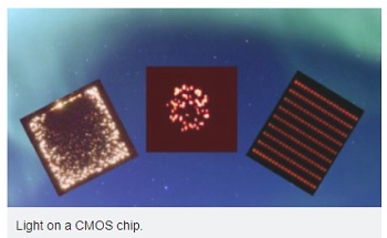
Electronics and light don't go well together on a standard 'CMOS' chip. Researcher Satadal Dutta of the University of Twente succeeded in introducing a light connection into the heart of a semiconductor chip. In this way, two circuits can communicate. Or: the worlds of electronics and photonics are connected.
What is particularly attractive about Dutta's solution is that no special materials or manufacturing processes are needed: the light comes from silicon. The light source, detector and the light channel can be made using the technology that is used to make the electronic circuits. Fully optical circuits are available nowadays, but they use materials like indium phosphide and gallium arsenide, which can't easily be combined with the CMOS chip processes used for semiconductor chips you'll find in today's smartphones, for example.
Avalanche LED
The alternative would be: make a LED out of silicon. And that's the problem: silicon only emits a tiny amount of infrared light, while a detector made out of silicon needs visible light. They are talking and listening at different wavelengths. Dutta therefore chooses a remarkable way out: connect the LED reverse. At low voltages, there's no current, but at a voltage that is high enough, there will be a small current that amplifies itself like an avalanche. In this 'avalanche mode', the LED will transmit visible light. Using the same process, the light detector, as well as the light channel in-between can be made. Thanks to the special comb structure that Dutta designed, the light source gets more uniform and energy efficient.
Isolation
An optical link on a chip is a good way to 'galvanically' isolate two circuits from each other. This is often necessary in cases where one circuit is a low-voltage and low-current one, while the other is a high-power circuit. They should be connected, but not by conducting wires, for reasons of safety. A classic transformer is an option then, but an optical connection is often used as well. Until now, this is a separate 'optocoupler', which is large and has a limited bit rate. Dutta's new solution is much more compact as an alternative: it total, it is just a few tens of microns and it offers the protection that's needed. Compared to optical channels in full-optical circuits, the energy consumption is relatively high, as there is quite some scattering of light. On the other hand: designing the electronics around the optical link in an efficient way, the amount of light needed for a successful connection, can be kept to a minimum.
Connecting worlds
All-optical circuits may become the 'new electronics', predictions say. In the transition from electronic to optic circuits, hybrid circuits, like the one Dutta designed, could play an important role.
Satadal Dutta (1990, Barrackpore, India) did his PhD research in the Semiconductor Components group of Prof Jurriaan Schmitz, together with the Integrated Circuit Design group of Prof. Bram Nauta. Dutta defended his thesis 'Avalanche-mode silicon LEDs for monolithic optical coupling in CMOS technology' on 8 November. It was supported financially by NWO-TTW in The Netherlands and by NXP Semiconductors.
Share on:


Suggested Items
Book Excerpt: The Printed Circuit Assembler’s Guide to... Factory Analytics
04/24/2024 | I-Connect007 Editorial TeamIn our fast-changing, deeply competitive, and margin-tight industry, factory analytics can be the key to unlocking untapped improvements to guarantee a thriving business. On top of that, electronics manufacturers are facing a tremendous burden to do more with less. If you don't already have a copy of this book, what follows is an excerpt from the introduction chapter of 'The Printed Circuit Assembler’s Guide to... Factory Analytics: Unlocking Efficiency Through Data Insights' to whet your appetite.
Listen Up! The Intricacies of PCB Drilling Detailed in New Podcast Episode
04/25/2024 | I-Connect007In episode 5 of the podcast series, On the Line With: Designing for Reality, Nolan Johnson and Matt Stevenson continue down the manufacturing process, this time focusing on the post-lamination drilling process for PCBs. Matt and Nolan delve into the intricacies of the PCB drilling process, highlighting the importance of hole quality, drill parameters, and design optimization to ensure smooth manufacturing. The conversation covers topics such as drill bit sizes, aspect ratios, vias, challenges in drilling, and ways to enhance efficiency in the drilling department.
Elevating PCB Design Engineering With IPC Programs
04/24/2024 | Cory Blaylock, IPCIn a monumental stride for the electronics manufacturing industry, IPC has successfully championed the recognition of the PCB Design Engineer as an official occupation by the U.S. Department of Labor (DOL). This pivotal achievement not only underscores the critical role of PCB design engineers within the technology landscape, but also marks the beginning of a transformative journey toward nurturing a robust, skilled workforce ready to propel our industry into the future.
Winner of The Science Show Rakett 69 Receives Incap Scholarship
04/24/2024 | IncapThe winner of the Rakett 69 science show, Andri Türkson, who stood out as an electronics enthusiast, received a scholarship from Incap Estonia, along with an internship opportunity in Saaremaa.
Alternative Manufacturing Inc. Awarded QML Requalification to IPC J-STD-001 and IPC-A-610
04/24/2024 | IPCIPC's Validation Services Program has awarded an IPC J-STD-001 and IPC-A-610 Qualified Manufacturers Listing (QML) requalification to Alternative Manufacturing Inc (AMI).