


 Marcy's Musings: The Growing Industry
 It’s Only Common Sense: Here’s What To Do After IPC APEX EXPO 2024
 Dan’s Biz Bookshelf: Seeing the How
NRL Improves Optical Efficiency in Nanophotonic Devices
January 5, 2018 | U.S. Naval Research LaboratoryEstimated reading time: 1 minute
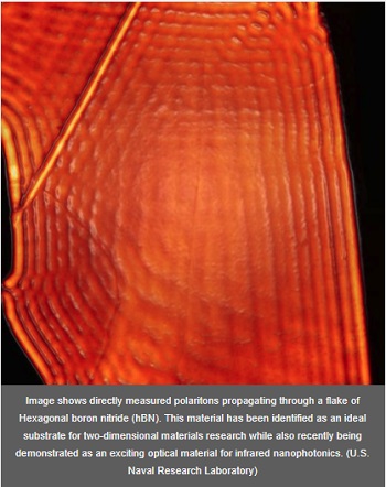
A team of physicists, headed by the U.S. Naval Research Laboratory (NRL), have demonstrated the means to improve the optical loss characteristics and transmission efficiency of hexagonal boron nitride devices, enabling very small lasers and nanoscale optics.
“The applications for this research are considerably broad,” said Dr. Alexander J. Giles, research physicist, NRL Electronics Science and Technology Division. “By confining light to very small dimensions, nanophotonic devices have direct applications for use in ultra-high resolution microscopes, solar energy harvesting, optical computing and targeted medical therapies.”
Hexagonal boron nitride (hBN) forms an atomically thin lattice consisting of boron and nitrogen atoms. This material has recently been demonstrated as an exciting optical material for infrared nanophotonics and is considered an ‘ideal substrate’ for two-dimensional materials.
While previous work demonstrated that natural hBN supports deeply sub-diffractional hyperbolic phonon polaritons desired for applications, such as, sub-diffractional optical imaging (so-called ‘hyperlensing’), energy conversion, chemical sensing, and quantum nanophotonics, limited transmission efficiencies continue to persist.
"We have demonstrated that the inherent efficiency limitations of nanophotonics can be overcome through the careful engineering of isotopes in polar semiconductors and dielectric materials,” Giles said.
Naturally occurring boron is comprised of two isotopes, boron-10 and boron-11, lending a 10 percent difference in atomic masses. This difference results in substantial losses due to phonon scattering, limiting the potential applications of this material. The research team at NRL has engineered greater than 99 percent isotopically pure samples of hBN, meaning they consist almost entirely of either boron-10 or boron-11 isotopes.
This approach results in a dramatic reduction in optical losses, resulting in optical modes that travel up to three times farther and persist for up to three times longer than natural hBN. These long-lived vibrational modes not only enable immediate advances specific to hBN — near field optics and chemical sensing — but also provide a strategic approach for other materials systems to exploit and build upon.
“Controlling and manipulating light at nanoscale, sub-diffractional dimensions is notoriously difficult and inefficient,” said Giles. “Our work represents a new path forward for the next generation of materials and devices.”
Contributors to this research include scientists from the University of California San Diego, Kansas State University, Oak Ridge National Laboratory, Columbia University, and Vanderbilt University. Full details of this research entitled “Ultralow-loss polaritons in isotopically pure boron nitride,” can be found in the December 11, 2017 edition of Nature Materials (doi:10.1038/nmat5047).
Share on:


Suggested Items
Groundbreaking Ceremony Marks the Beginning of a New Era for Newccess Industrial; The Construction of the MINGXIN Building
04/12/2024 | Newccess IndustrialOn a clear and sunny day in March, the groundbreaking ceremony for the MINGXIN Building took place in Shenzhen, China. This moment marked the official commencement of construction for a project that will reshape the semiconductor materials industry.
The Need for a Holistic Global Sustainability Standard
04/10/2024 | Michael Ford, Aegis SoftwareNo one can deny that the resources of our fragile planet are finite. The environment seems like a third party, subject to constant degradation. We’re acutely aware of the effects of pollution on our climate, and despite our “throw-away” culture, recycling and recovery of materials has remained relatively expensive, even as we use more energy just to survive.
iNEMI Publishes Four Roadmap Topics
04/04/2024 | iNEMIThe International Electronics Manufacturing Initiative (iNEMI) announces the availability of the first roadmap topics in the new iNEMI Roadmap format. Printed circuit boards, sustainable electronics, smart manufacturing, and mmWave materials and test are now available online.
Insulectro’s 'Storekeepers' Extend Their Welcome to Technology Village at IPC APEX EXPO
04/03/2024 | InsulectroInsulectro, the largest distributor of materials for use in the manufacture of PCBs and printed electronics, welcomes attendees to its TECHNOLOGY VILLAGE during this year’s IPC APEX EXPO at the Anaheim Convention Center, April 9-11, 2024.
Checking In With ICAPE Group
04/03/2024 | Nolan Johnson, I-Connect007ICAPE Group’s field application engineer Erik Pederson drills down on sustainability, supply chain resiliency, and what value engineering really looks like in this exclusive interview. Founded in 1999, European-based ICAPE Group provides 21 million printed circuit boards and over six million technical parts to manufacturers every month. With 30 PCB manufacturing partners globally and 50 partners providing a wide array of technical parts, ICAPE Group has operations in China, Taiwan, Thailand, South Korea, Vietnam, South Africa, Europe, Mexico, and the United States. The company also focuses on the value proposition for its customers.