


 Marcy's Musings: The Growing Industry
 It’s Only Common Sense: Here’s What To Do After IPC APEX EXPO 2024
 Dan’s Biz Bookshelf: Seeing the How
Scientists Develop Topological Defect Detection Method
April 5, 2018 | ITMO UniversityEstimated reading time: 3 minutes
An international scientific team has developed a new method of probing topological structures and their topological phase transitions. The method is based on examining the reflection spectrum of EM-waves reflecting off an object from different impact angles. The accuracy of the method’s results has been verified experimentally in both IR and microwave spectra.
Topology is an area of mathematics that studies the properties of objects that remain unchanged despite the objects’ constant deformation. From a topological point of view, a doughnut and a mug are the same since they both have a hole in the center. Topological invariants lie at the core of many important observable properties of matter. They are incorporated in the creation of new, unusual materials, which are used, for example, to control light propagation in optical systems.
To detect topologically non-trivial structures, scientists usually scan the propagation of an object’s near-field. In other words, they monitor an object’s emissions at a distance much smaller than a wavelength. The resulting near-field map lets them draw conclusions about the topology of the object’s photonic bands. For instance, it is possible to determine if the object contains any topological edge states, and to what degree they are protected from scattering in areas with defects or non-uniformity.
Scientists from ITMO University together with their colleagues from the City University of New York have proposed a new method of topological analysis based on spectroscopy of an object’s far-field.
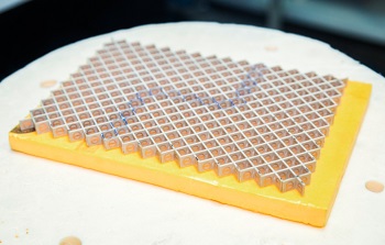
“We posed the question: do the topological properties of a system affect how it disperses light at long distances? – explains , research fellow at ITMO’s Metamaterials Laboratory, – To answer it, our colleagues, led by Alexander Khanikaev, developed and manufactured two two-dimensional structures using silicon cylinders of slightly different geometric parameters. One was trivial, and the other topological”.
Making such structures isn’t easy, say the scientists. For that, they need to use the latest nanofabrication methods. Having analyzed the resulting samples’ spectra, they developed a theoretical model depicting the results of the analysis. It allowed them to determine the structure’s topological invariant. This model later became the basis for the far-field spectroscopy method.
“At some point, our reviewers expressed interest in whether we can confirm that the results we got through far-field analysis are in line with the standard technique of near-field analysis. To do that, we conducted a microwave experiment. We created a metasurface of two parts: one topologically trivial and one non-trivial. Our goal was to observe the topological state localized on the border of these two parts. In the end, we managed to produce an all-dielectric metasurface which contains topologically-protected states in the microwave band. At the same time, the polarization of the edge state turned out to be unequivocally connected to the direction of its propagation. The experiment confirmed the accuracy of our model, and the article was accepted”, - adds , PhD student at ITMO’s Faculty of Physics and Engineering.
The new method’s advantage is that it lets researchers study the topology of objects from a distance.
“We no longer need to examine the propagation field right on the surface of the structure. We can now detect unusual topological states in materials from afar. In addition, as we developed the method, we proved that while energy loss can occur in topological structures, topological edge states still persist, – notes Maxim Gorlach. – We are now planning to use the new method to study three-dimensional topological insulators and we’re expecting some new and exciting results”.
Earlier on, topological states were only suggested for use in secure signal transmission. But now, explain the scientists, the range of applications is becoming much wider
“It is known that nanofabrication methods are limited in precision due to various technological reasons – and photonic nanostructures are guaranteed to contain defects. This leads to loss of efficiency and accuracy of the devices produced with these methods. For example, any biosensor made using nanofabrication methods will be limited in the accuracy of its measurements, all due to the defects. Using topological states in the construction of these detectors, we can increase their sensitivity and precision – even despite the presence of structural defects,” – says project lead Alexander Khanikaev.
Share on:


Suggested Items
DOCOMO to Collaborate with AT&T, Verizon and Jio for Open RAN Verifications
02/15/2024 | JCN NewswireNTT DOCOMO, INC. announced today that it will participate in Open RAN verifications in the United States as the ACCoRD (Acceleration of Compatibility and Commercialization for Open RAN Deployments) project in a consortium jointly founded with AT&T Inc. (AT&T), Verizon Communications Inc. (Verizon), and Reliance Jio Infocomm Ltd. (Jio).
AUKUS Defense Scientists Test Robotic Vehicles
02/06/2024 | U.S. DoDDefense scientists from Australia, the United Kingdom and the United States collaboratively tested a range of robotic vehicles and their sensors during a trial at Cultana Training Area, South Australia. The Trusted Operation of Robotic Vehicles in a Contested Environment (TORVICE) trial was conducted in fall 2023 to identify and resolve vulnerabilities faced by autonomous systems in a congested electronic warfare environment.
Material Insight: A Conversation with Congressman Blake Moore
11/28/2023 | Dr. Preeya Kuray -- Column: Material InsightOn May 11, 2023, Reps. Blake Moore (R-UT) and Anna Eshoo (D-CA) introduced the Protecting Circuit Boards and Substrates (PCB) Act to Congress. In October, I had the great pleasure of discussing the bipartisan Protecting Circuit Boards and Substrates Act with Congressman Moore, who represents Utah’s First Congressional District. He shared his thoughts on how supporting and investing in the domestic PCB industry can help bolster American security.
Rheinmetall's Next-generation Simulation Solution Wins Backing from European Union
10/24/2023 | RheinmetallCoordinated and led by Rheinmetall, the FEDERATES consortium, which stands for Federated Ecosystem of European Simulation Assets for Training and Decision Support, has been selected by the European Union for €30 million in funding.
U.S. Army 4-Star General (Ret.) Michael X. Garrett Appointed to Nano Dimension’s Board of Directors
10/17/2023 | Nano DimensionNano Dimension Ltd., a leading supplier of Additively Manufactured Electronics and multi-dimensional polymer, metal & ceramic Additive Manufacturing 3D printers, today announced that 4-Star General (Ret.) Michael X. Garrett has been appointed as a member of its Board of Directors, effective as of October 15th, 2023.