


 Flexible Thinking: PCB Designers Still Wanted
 Connect the Dots: Five Best Practices for Designing Flex and Rigid-flex PCBs
 Tim’s Takeaways: Human Ingenuity and the Rigid-flex PCB
Atotech to Introduce Cupracid Flex and InPro Flex
June 13, 2018 | AtotechEstimated reading time: 2 minutes
The flex/ flex-rigid PCB market continues to grow as more and more designs call for flexible inner layers with ever finer lines and spaces. At the same time, the need for high volume reel to reel formats as well as pattern plating with lower base copper thickness drives the FPCB market.
As one of the market leaders for BMV filling and through hole filling in the IC-substrate market, Atotech has developed two new acid copper processes – InPro Flex and Cupracid Flex – to serve the flexible printed circuit board market and support its customers to overcome the current technical barriers in FPCB manufacturing.
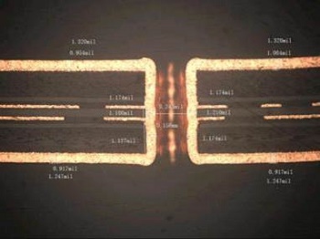
Excellent throwing power: Board thickness: 0.3mm, Hole: 0.15mm, CD: 2.8ASD, Line speed: 0.6m/min, Flow rate: 15HZ, Average TP% : 120%
Cupracid Flex and InPro Flex
“Cupracid Flex and InPro Flex are specifically designed for standard conformal flex and rigid-flex applications. While the Cupracid Flex process is for use in vertical systems with soluble anodes, InPro® Flex can be used in systems with insoluble anodes,” states Mustafa Oezkoek, Global Product Manager Panel and Pattern Plating at Atotech Deutschland GmbH.
The simple two additive processes can be analyzed by standard CVS method and are suitable for vertical equipment or vertical reel to reel equipment with educator or sparger systems. They can be operated in panel and pattern plating and provide excellent line shape, outstanding crystal structure and a ductility of more than 23% in either manufacturing method.
Features and Benefits
“Cupracid Flex and InPro Flex are highly reliable processes and deliver excellent physical properties,” continues Mustafa. “Both solutions assure first-rate throwing power at high current densities without any corner flattening. At the same time, pattern uniformity and line shape are very good. And, according to IPC, the bending performance is exceptional.”
Both products have been rolled out globally and are available worldwide.
About Atotech
Atotech is one of the world’s leading manufacturers of specialty chemicals and equipment for the printed circuit board, IC-substrate and semiconductor industries, as well as for the decorative and functional surface finishing industries. Atotech has annual sales of USD1.2 billion (2017). The company is fully committed to sustainability – we develop technologies to minimize waste and to reduce environmental impact. Atotech has its headquarters in Berlin, Germany, and employs about 4,000 people in over 40 countries. About a quarter of all staff works in one of the four locations in Germany: Berlin, Feucht, Neuruppin, and Trebur. For more information, click here.
Share on:


Suggested Items
Insulectro’s 'Storekeepers' Extend Their Welcome to Technology Village at IPC APEX EXPO
04/03/2024 | InsulectroInsulectro, the largest distributor of materials for use in the manufacture of PCBs and printed electronics, welcomes attendees to its TECHNOLOGY VILLAGE during this year’s IPC APEX EXPO at the Anaheim Convention Center, April 9-11, 2024.
ENNOVI Introduces a New Flexible Circuit Production Process for Low Voltage Connectivity in EV Battery Cell Contacting Systems
04/03/2024 | PRNewswireENNOVI, a mobility electrification solutions partner, introduces a more advanced and sustainable way of producing flexible circuits for low voltage signals in electric vehicle (EV) battery cell contacting systems.
Heavy Copper PCBs: Bridging the Gap Between Design and Fabrication, Part 1
04/01/2024 | Yash Sutariya, Saturn Electronics ServicesThey call me Sparky. This is due to my talent for getting shocked by a variety of voltages and because I cannot seem to keep my hands out of power control cabinets. While I do not have the time to throw the knife switch to the off position, that doesn’t stop me from sticking screwdrivers into the fuse boxes. In all honesty, I’m lucky to be alive. Fortunately, I also have a talent for building high-voltage heavy copper circuit boards. Since this is where I spend most of my time, I can guide you through some potential design for manufacturability (DFM) hazards you may encounter with heavy copper design.
Trouble in Your Tank: Supporting IC Substrates and Advanced Packaging, Part 5
03/19/2024 | Michael Carano -- Column: Trouble in Your TankDirect metallization systems based on conductive graphite or carbon dispersion are quickly gaining acceptance worldwide. Indeed, the environmental and productivity gains one can achieve with these processes are outstanding. In today’s highly competitive and litigious environment, direct metallization reduces costs associated with compliance, waste treatment, and legal issues related to chemical exposure. What makes these processes leaders in the direct metallization space?
AT&S Shines with Purest Copper on World Recycling Day
03/18/2024 | AT&SThe Styrian microelectronics specialist AT&S is taking World Recycling Day as an opportunity to review the progress that has been made in recent months at its sites around the world in terms of the efficient use of resources: