


 It’s Only Common Sense: OCCAM—the Time Is Now
 Marcy's Musings: The Growing Industry
 Dan’s Biz Bookshelf: Seeing the How
Researchers Develop UV Narrow-band Photodetector Based on Indium Oxide Nanocrystals
July 6, 2018 | Lobachevsky State University of Nizhni NovgorodEstimated reading time: 1 minute
Semiconductor quantum dots (nanocrystals just a few nanometers in size) have attracted researchers’ attention due to the size dependent effects that determine their novel electrical and optical properties. By changing the size of such objects, it is possible to adjust the wavelength of the emission they absorb, thus implementing selective photodetectors, including those for UV radiation.
Narrow-band UV photodetectors find application in many areas, in particular in biomedicine where they are used for fluorescence detection or UV phototherapy. The materials commonly used in the manufacture of such photoreceivers are wide-bandgap oxides and nitrides, which offer a greater range of operating temperatures and transparency for visible and solar light in addition to a smaller size of the device.
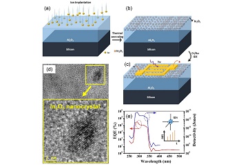
Indium oxide (In2O3) is a transparent wide-bandgap semiconductor oxide with a direct band gap of about 3.6 eV and an indirect band gap of ~ 2.5 eV. It is well known that highly sensitive UV photodetectors can be created based on In2O3.
According to Alexey Mikhaylov, head of the laboratory at the UNN Research Institute of Physics and Technology, researchers together with their Indian colleagues from Indian Institute of Technology Jodhpur and Indian Institute of Technology Ropar managed to synthesize In2O3 nanocrystals in an aluminum oxide (Al2O3) film on silicon by implanting indium ions.
Ion implantation is a basic method in modern electronic technology, which makes it possible to control the size of inclusions thus allowing the optical properties of the photodetector to be tuned. The Al2O3 matrix used for indium oxide nanocrystals offers some advantages over other dielectrics in that this wide-bandgap material (8.9 eV) is transparent for a wide range of wavelengths.
"In the process of our work, we managed to achieve a significant reduction in the dark current (more than two times as compared to a similar photodetector based on In2O3 nanowires). By integrating the In2O3 phase into the wide-band matrix and due to its low dark current, the new photodetector shows record values of the responsivity and external quantum efficiency," Alexey Mikhaylov notes.
The sensitivity band in the UV range has a width of only 60 nm and shows a high UV-visible rejection ratio (up to 8400). This photodetector is highly suitable for practical applications such as narrow-band spectrum-selective photodetectors. The device design based on ion-synthesized nanocrystals could provide a new approach for realizing a visible-blind photodetector.
Share on:


Suggested Items
Koh Young Showcases Award-winning Inspection Solutions at SMTconnect with SmartRep in Hall 4A.225
04/25/2024 | Koh Young TechnologyKoh Young Technology, the industry leader in True 3D measurement-based inspection solutions, will showcase an array of award-winning inspection and measurement solutions at SMTconnect alongside its sales partner, SmartRep, in booth 4A.225 at NürnbergMesse from June 11-13, 2023. The following offers a glimpse into what Koh Young will present at the tradeshow:
Real Time with… IPC APEX EXPO 2024: Plasmatreat: Innovative Surface Preparation Solutions
04/25/2024 | Real Time with...IPC APEX EXPOIn this interview, Editor Nolan Johnson speaks with Hardev Grewal, CEO and president of Plasmatreat, a developer of atmospheric plasma solutions. Plasmatreat uses clean compressed air and electricity to create plasma, offering environmentally friendly methods for surface preparation. Their technology measures plasma density for process optimization and can remove organic micro-contamination. Nolan and Hardev also discuss REDOX-Tool, a new technology for removing metal oxides.
Nanotechnology Market to Surpass $53.51 Billion by 2031
04/25/2024 | PRNewswireSkyQuest projects that the nanotechnology market will attain a value of USD 53.51 billion by 2031, with a CAGR of 36.4% over the forecast period (2024-2031).
Cadence, TSMC Collaborate on Wide-Ranging Innovations to Transform System and Semiconductor Design
04/25/2024 | Cadence Design SystemsCadence Design Systems, Inc. and TSMC have extended their longstanding collaboration by announcing a broad range of innovative technology advancements to accelerate design, including developments ranging from 3D-IC and advanced process nodes to design IP and photonics.
SMC Korea 2024 to Highlight Semiconductor Materials Trends and Innovations on Industry’s Path to $1 Trillion
04/24/2024 | SEMIWith Korea a major consumer of semiconductor materials and advanced materials a key driver of innovation on the industry’s path to $1 trillion, industry leaders and experts will gather at SMC (Strategic Materials Conference) Korea 2024 on May 29 at the Suwon Convention Center in Gyeonggi-do, South Korea to provide insights into the latest materials developments and trends. Registration is open.