


 Marcy's Musings: The Growing Industry
 It’s Only Common Sense: Here’s What To Do After IPC APEX EXPO 2024
 Dan’s Biz Bookshelf: Seeing the How
Kirigami-Inspired Technique Manipulates Light At The Nanoscale
July 9, 2018 | MITEstimated reading time: 3 minutes
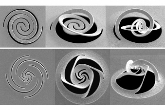
Nanokirigami has taken off as a field of research in the last few years; the approach is based on the ancient arts of origami (making 3-D shapes by folding paper) and kirigami (which allows cutting as well as folding) but applied to flat materials at the nanoscale, measured in billionths of a meter.
Now, researchers at MIT and in China have for the first time applied this approach to the creation of nanodevices to manipulate light, potentially opening up new possibilities for research and, ultimately, the creation of new light-based communications, detection, or computational devices.
The findings are described today in the journal Science Advances, in a paper by MIT professor of mechanical engineering Nicholas X Fang and five others. Using methods based on standard microchip manufacturing technology, Fang and his team used a focused ion beam to make a precise pattern of slits in a metal foil just a few tens of nanometers thick. The process causes the foil to bend and twist itself into a complex three-dimensional shape capable of selectively filtering out light with a particular polarization.
Previous attempts to create functional kirigami devices have used more complicated fabrication methods that require a series of folding steps and have been primarily aimed at mechanical rather than optical functions, Fang says. The new nanodevices, by contrast, can be formed in a single folding step and could be used to perform a number of different optical functions.
For these initial proof-of-concept devices, the team produced a nanomechanical equivalent of specialized dichroic filters that can filter out circularly polarized light that is either “right-handed” or “left-handed.” To do so, they created a pattern just a few hundred nanometers across in the thin metal foil; the result resembles pinwheel blades, with a twist in one direction that selects the corresponding twist of light.
The twisting and bending of the foil happens because of stresses introduced by the same ion beam that slices through the metal. When using ion beams with low dosages, many vacancies are created, and some of the ions end up lodged in the crystal lattice of the metal, pushing the lattice out of shape and creating strong stresses that induce the bending.
“We cut the material with an ion beam instead of scissors, by writing the focused ion beam across this metal sheet with a prescribed pattern,” Fang says. “So you end up with this metal ribbon that is wrinkling up” in the precisely planned pattern.
“It’s a very nice connection of the two fields, mechanics and optics,” Fang says. The team used helical patterns to separate out the clockwise and counterclockwise polarized portions of a light beam, which may represent “a brand new direction” for nanokirigami research, he says.
The technique is straightforward enough that, with the equations the team developed, researchers should now be able to calculate backward from a desired set of optical characteristics and produce the needed pattern of slits and folds to produce just that effect, Fang says.
“It allows a prediction based on optical functionalities” to create patterns that achieve the desired result, he adds. “Previously, people were always trying to cut by intuition” to create kirigami patterns for a particular desired outcome.
The research is still at an early stage, Fang points out, so more research will be needed on possible applications. But these devices are orders of magnitude smaller than conventional counterparts that perform the same optical functions, so these advances could lead to more complex optical chips for sensing, computation, or communications systems or biomedical devices, the team says.
For example, Fang says, devices to measure glucose levels often use measurements of light polarity, because glucose molecules exist in both right- and left-handed forms which interact differently with light. “When you pass light through the solution, you can see the concentration of one version of the molecule, as opposed to the mixture of both,” Fang explains, and this method could allow for much smaller, more efficient detectors.
Circular polarization is also a method used to allow multiple laser beams to travel through a fiber-optic cable without interfering with each other. “People have been looking for such a system for laser optical communications systems” to separate the beams in devices called optical isolaters, Fang says. “We have shown that it’s possible to make them in nanometer sizes.”
The team also included MIT graduate student Huifeng Du; Zhiguang Liu, Jiafang Li (project supervisor), and Ling Lu at the Chinese Academy of Sciences in Beijing; and Zhi-Yuan Li at the South China University of Technology. The work was supported by the National Key R&D Program of China, the National Natural Science Foundation of China, and the U.S Air Force Office of Scientific Research.
Share on:


Suggested Items
Water Management in a Large Printed Circuit Board Manufacturer
04/15/2024 | Charles Nehrig, TTM TechnologiesTTM’s environmental management is grounded in its Environmental Statement and Environmental Policy, which promote measures that make for a more responsible environmental management process. Our management system helps TTM work toward minimizing its environmental footprint and increasing the sustainability of its operations. TTM monitors its environmental performance just as it monitors its operational performance, and provides the resources required to adhere to the Company’s environmental responsibilities.
Happy’s Tech Talk #27: Integrated Mesh Power System (IMPS) for PCBs
04/08/2024 | Happy Holden -- Column: Happy’s Tech TalkA significant decrease in HDI substrate production cost can be achieved by reducing the number of substrate layers from conventional through-hole multilayers and microvia multilayers of eight, 10, 12, and more to only two layers. Besides reducing direct processing steps, the yield will increase as defect-producing operations are eliminated. The integrated mesh power system (IMPS) was invented in the latter years of MCM-D use for thin-film fabrication. Those geometries fit today into our use of ultra HDI.
Trouble in Your Tank: Supporting IC Substrates and Advanced Packaging, Part 5
03/19/2024 | Michael Carano -- Column: Trouble in Your TankDirect metallization systems based on conductive graphite or carbon dispersion are quickly gaining acceptance worldwide. Indeed, the environmental and productivity gains one can achieve with these processes are outstanding. In today’s highly competitive and litigious environment, direct metallization reduces costs associated with compliance, waste treatment, and legal issues related to chemical exposure. What makes these processes leaders in the direct metallization space?
Indium Corporation Experts to Present at SEMI THERM
03/07/2024 | Indium CorporationIndium Corporation Global Account Manager and Senior Thermal Technologist Tim Jensen and Product Development Specialist for Thermal Interface Materials Miloš Lazić will present on thermal interface material (TIM) technology at SEMI-THERM, taking place March 25–28 in San Jose, California, U.S.
Indium Corporation to Showcase Proven EV Products and High-Reliability Alloys at Productronica China
02/28/2024 | Indium CorporationAs a materials pioneer and trusted partner in electric vehicle (EV) and e-Mobility manufacturing, Indium Corporation is proud to showcase its high-reliability alloys and soldering solutions at Productronica China, March 20-22, in Shanghai.