


 It’s Only Common Sense: OCCAM—the Time Is Now
 Marcy's Musings: The Growing Industry
 Dan’s Biz Bookshelf: Seeing the How
New Semiconducting Crystal Rivals Diamond for Heat Conductivity
July 12, 2018 | University of Texas at AustinEstimated reading time: 3 minutes
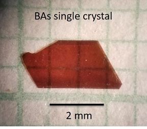
The need for faster and smaller electronics has resulted in microelectronic components that produce progressively more heat. Thus, heat dissipation is an important issue, and one solution for cooling is to develop novel semiconducting materials with high thermal conductivity.
Fragment of boron arsenide crystal under a microscope.Engineers and scientists have long known that diamond is the best material for conducting heat, but it has its drawbacks — the most obvious being that it is quite costly. It is also an electrical insulator. In addition, when paired with a semiconductor device, diamond expands at a different rate than the device does when it is heated.
Now, a group of engineers from the Cockrell School of Engineering at The University of Texas at Austin, along with research partners across Texas and the U.S., has found a crystal material from two relatively common elements — boron and arsenic — that demonstrates far higher thermal conductivity than any other semiconductors and metals currently in use, such as silicon, silicon carbide, copper and silver.
The team’s discovery, which was published in the July 5 issue of Science, could offer a more viable alternative to diamond for addressing a range of technological challenges, including cooling electronic devices and nanodevices.
Thermal conductivity is measured in the unit of Wm-1K-1, used to denote the amount of heat flux that can pass through a material that is 1 meter long when the temperature difference from one side to the other is 1 Kelvin. The boron arsenide crystals have a conductivity about 1,000 Wm-1K-1 at room temperature, the researchers reported.
Copper, by comparison, has a conductivity of about 400 Wm-1K-1, and diamond has a reported thermal conductivity of 2,000 Wm-1K-1 at room temperature.
The crystals were grown by a team led by professor Zhifeng Ren at the University of Houston. The high thermal conductivity was validated by the Cockrell School’s team and another team led by professor Gang Chen at MIT. The UT Austin team includes post-doc fellows Xi Chen and Jaehyun Kim, graduate students Sean Sullivan and Yuanyuan Zhou and professors Jianshi Zhou and Li Shi from the Cockrell School’s Department of Mechanical Engineering and Texas Materials Institute.
It is difficult to measure the thermal conductivity accurately when the value is high, because the temperature gradient is very small. When the boron arsenide crystals were measured using a tightly focused laser beam, the measured thermal conductivity values varied across different locations of the same sample. To address the problem, the UT Austin team devised two different sensitive methods to measure the average thermal conductivity of the entire bulk crystal.
“With these methods, we have confirmed that the average bulk thermal conductivity reaches impressive levels at room temperature,” said Chen, one of the post-docs on the project. “The obtained temperature dependence of thermal conductivity also reveals unique thermal transport mechanisms.”
Team member Sean Sullivan, a Ph.D. candidate in UT materials science and engineering said the unique thing about boron arsenide is that it is the only semiconductor that we know of with high thermal conductivity.
“It breaks long-held criteria thought to be critical for developing materials with superior thermal transport characteristics,” Sullivan said.
The experiments have been motivated by a theoretical prediction from professor David Broido at Boston College along with Lucas Lindsay and Tom Reinecke at the Naval Research Lab. The team’s discovery is an important step toward future applications and uses of boron arsenide.
The next step, said the Cockrell School’s Li Shi, will be “to explore device technologies with the boron arsenide bulk crystals.”
The project was funded by the U.S. Navy’s Multidisciplinary University Research Initiative (MURI). The MURI team is led by Shi and includes researchers from the University of Houston, Boston College, UT Austin, MIT, the University of Illinois Urbana-Champaign and the University of California, Los Angeles.
Share on:


Suggested Items
Designer’s Notebook: What Designers Need to Know About Manufacturing, Part 2
04/24/2024 | Vern Solberg -- Column: Designer's NotebookThe printed circuit board (PCB) is the primary base element for providing the interconnect platform for mounting and electrically joining electronic components. When assessing PCB design complexity, first consider the component area and board area ratio. If the surface area for the component interface is restricted, it may justify adopting multilayer or multilayer sequential buildup (SBU) PCB fabrication to enable a more efficient sub-surface circuit interconnect.
Insulectro’s 'Storekeepers' Extend Their Welcome to Technology Village at IPC APEX EXPO
04/03/2024 | InsulectroInsulectro, the largest distributor of materials for use in the manufacture of PCBs and printed electronics, welcomes attendees to its TECHNOLOGY VILLAGE during this year’s IPC APEX EXPO at the Anaheim Convention Center, April 9-11, 2024.
ENNOVI Introduces a New Flexible Circuit Production Process for Low Voltage Connectivity in EV Battery Cell Contacting Systems
04/03/2024 | PRNewswireENNOVI, a mobility electrification solutions partner, introduces a more advanced and sustainable way of producing flexible circuits for low voltage signals in electric vehicle (EV) battery cell contacting systems.
Heavy Copper PCBs: Bridging the Gap Between Design and Fabrication, Part 1
04/01/2024 | Yash Sutariya, Saturn Electronics ServicesThey call me Sparky. This is due to my talent for getting shocked by a variety of voltages and because I cannot seem to keep my hands out of power control cabinets. While I do not have the time to throw the knife switch to the off position, that doesn’t stop me from sticking screwdrivers into the fuse boxes. In all honesty, I’m lucky to be alive. Fortunately, I also have a talent for building high-voltage heavy copper circuit boards. Since this is where I spend most of my time, I can guide you through some potential design for manufacturability (DFM) hazards you may encounter with heavy copper design.
Trouble in Your Tank: Supporting IC Substrates and Advanced Packaging, Part 5
03/19/2024 | Michael Carano -- Column: Trouble in Your TankDirect metallization systems based on conductive graphite or carbon dispersion are quickly gaining acceptance worldwide. Indeed, the environmental and productivity gains one can achieve with these processes are outstanding. In today’s highly competitive and litigious environment, direct metallization reduces costs associated with compliance, waste treatment, and legal issues related to chemical exposure. What makes these processes leaders in the direct metallization space?