


 Marcy's Musings: The Growing Industry
 It’s Only Common Sense: Here’s What To Do After IPC APEX EXPO 2024
 Dan’s Biz Bookshelf: Seeing the How
Researchers Improve Conductive Property of Graphene, Advancing Promise of Solar Technology
July 12, 2018 | The University of KansasEstimated reading time: 4 minutes
In 2010, the Nobel Prize in Physics went to the discoverers of graphene. A single layer of carbon atoms, graphene possesses properties that are ideal for a host of applications. Among researchers, graphene has been the hottest material for a decade. In 2017 alone, more than 30,000 research papers on graphene were published worldwide.
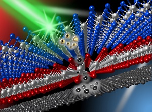
Image: Researchers from the University of Kansas have connected a graphene layer with two other atomic layers (molybdenum diselenide and tungsten disulfide), thereby extending the lifetime of excited electrons in graphene by several hundred times. Credit: Matthew Bellus.
Now, two researchers from the University of Kansas, Professor Hui Zhao and graduate student Samuel Lane, both of the Department of Physics & Astronomy, have connected a graphene layer with two other atomic layers (molybdenum diselenide and tungsten disulfide) thereby extending the lifetime of excited electrons in graphene by several hundred times. The finding will be published on Nano Futures, a newly launched and highly selective journal.
The work at KU may speed development of ultrathin and flexible solar cells with high efficiency.
For electronic and optoelectronic applications, graphene has excellent charge transport property. According to the researchers, electrons move in graphene at a speed of 1/30 of the speed of light — much faster than other materials. This might suggest that graphene can be used for solar cells, which convert energy from sunlight to electricity. But graphene has a major drawback that hinders such applications – its ultrashort lifetime of excited electrons (that is, the time an electron stays mobile) of only about one picosecond (one-millionth of one-millionth of a second, or 10-12 second).
“These excited electrons are like students who stand up from their seats — after an energy drink, for example, which activates students like sunlight activates electrons,” Zhao said. “The energized students move freely in the classroom — like human electric current.”
The KU researcher said one of the biggest challenges to achieving high efficiency in solar cells with graphene as the working material is that liberated electrons — or, the standing students — have a strong tendency to losing their energy and become immobile, like students sitting back down.
“The number of electrons, or students from our example, who can contribute to the current is determined by the average time they can stay mobile after they are liberated by light,” Zhao said. “In graphene, an electron stays free for only one picosecond. This is too short for accumulating a large number of mobile electrons. This is an intrinsic property of graphene and has been a big limiting factor for applying this material in photovoltaic or photo-sensing devices. In other words, although electrons in graphene can become mobile by light excitation and can move quickly, they only stay mobile too short a time to contribute to electricity.”
In their new paper, Zhao and Lane report this issue could be solved by using the so-called van der Waals materials. The principle of their approach is rather simple to understand.
“We basically took the chairs away from the standing students so that they have nowhere to sit,” Zhao said. “This forces the electrons to stay mobile for a time that is several hundred times longer than before.”
To achieve this goal, working in KU’s Ultrafast Laser Lab, they designed a tri-layer material by putting single layers of MoSe2, WS2 and graphene on top of each other.
“We can think of the MoSe2 and graphene layers as two classrooms full of students all sitting, while the middle WS2 layer acts as a hallway separating the two rooms,” Zhao said. “When light strikes the sample, some of the electrons in MoSe2 are liberated. They are allowed to go across the WS2-layer hallway to enter the other room, which is graphene. However, the hallway is carefully designed so that the electrons have to leave their seats in MoSe2. Once in graphene, they have no choice but to stay mobile and hence contribute to electric currents, because their seats are no longer available to them.”
To demonstrate that the idea works, the KU researchers used an ultrashort laser pulse (0.1 picosecond) to liberate some of the electrons in MoSe2. By using another ultrashort laser pulse, they were able to monitor these electrons as they move to graphene. They found that these electrons move through the “hallway” in about 0.5 picosecond on average. They then stay mobile for about 400 picoseconds — a 400-fold improvement than a single layer of graphene, which they also measured in the same study.
The researchers also confirm “seats” left in MoSe2 also stay unoccupied for the same amount of time. In the classical world, these seats should stay empty forever. In quantum mechanics, however, the electrons “tunnel” back to these seats. The researchers propose this process determined the lifetime of the mobile electrons. So, by choosing different “hallway” layers, this time can be controlled for various applications.
The research was funded by National Science Foundation. Lane is supported by Self Graduate Fellowship.
Share on:


Suggested Items
Happy’s Tech Talk #27: Integrated Mesh Power System (IMPS) for PCBs
04/08/2024 | Happy Holden -- Column: Happy’s Tech TalkA significant decrease in HDI substrate production cost can be achieved by reducing the number of substrate layers from conventional through-hole multilayers and microvia multilayers of eight, 10, 12, and more to only two layers. Besides reducing direct processing steps, the yield will increase as defect-producing operations are eliminated. The integrated mesh power system (IMPS) was invented in the latter years of MCM-D use for thin-film fabrication. Those geometries fit today into our use of ultra HDI.
Insulectro’s 'Storekeepers' Extend Their Welcome to Technology Village at IPC APEX EXPO
04/03/2024 | InsulectroInsulectro, the largest distributor of materials for use in the manufacture of PCBs and printed electronics, welcomes attendees to its TECHNOLOGY VILLAGE during this year’s IPC APEX EXPO at the Anaheim Convention Center, April 9-11, 2024.
Now Available: Episode 4, Season 2 of Designing for Reality—Lamination
04/04/2024 | I-Connect007I-Connect007 has just released the latest episode of its podcast series, On the Line With..., which focuses on designing for reality in the electronics industry. Multilayer boards bring along a completely different set of processes. In this installment, ASC Sunstone VP/Manager Matt Stevenson discusses manufacturing techniques for multilayer boards. Of course, this necessitates a review of drill and registration techniques, followed by the ins and outs of lamination.
Heavy Copper PCBs: Bridging the Gap Between Design and Fabrication, Part 1
04/01/2024 | Yash Sutariya, Saturn Electronics ServicesThey call me Sparky. This is due to my talent for getting shocked by a variety of voltages and because I cannot seem to keep my hands out of power control cabinets. While I do not have the time to throw the knife switch to the off position, that doesn’t stop me from sticking screwdrivers into the fuse boxes. In all honesty, I’m lucky to be alive. Fortunately, I also have a talent for building high-voltage heavy copper circuit boards. Since this is where I spend most of my time, I can guide you through some potential design for manufacturability (DFM) hazards you may encounter with heavy copper design.
Kioxia, WD Elevate Capacity Utilization, Pushing NAND Flash Supply Growth to 10.9%
03/19/2024 | TrendForceTrendForce reports that anticipation of NAND Flash price hikes into Q2 has motivated certain suppliers to minimize losses and lower costs in hopes of returning to profitability this year.