


 It’s Only Common Sense: OCCAM—the Time Is Now
 Marcy's Musings: The Growing Industry
 Dan’s Biz Bookshelf: Seeing the How
Nanocrystal Links Could Lead to Better Electronics
July 17, 2018 | University of ChicagoEstimated reading time: 2 minutes
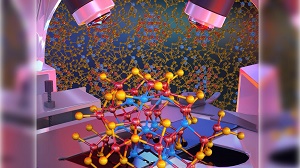
Chemists and engineers today are very interested in a kind of nanotechnology enabled by tiny islands of nanoparticles called “colloidal nanocrystals.” They can be made out of abundant and non-toxic materials, and they can be easily tweaked to have a number of different properties as a function of their size. Depending on how they’re built, colloidal nanocrystals could be made into solar panels, electronics or optical devices. But all of these applications require making nanocrystals friendly places for electrons to travel along.
A new study published in Nature Nanotechnology helps fill in the cracks for scientists trying to use nanocrystals to design better electronic and optoelectronic devices. According to research by University of Chicago, Argonne National Laboratory and Max Planck Institute for Iron Research scientists, inorganic links between the nanoparticles themselves are changing and reforming on the surface of the nanoparticles.
The team focused on the links between nanoparticles. At first, scientists used organic molecules to link them, but these tended to block the movement of electrons. Some recent experiments have seen much better results for inorganic molecules instead, but no one was sure why. “We never had an atomistic model for the behavior of these inorganic linkers,” said study co-author Giulia Galli, the Liew Family Professor of Molecular Engineering and professor of chemistry at the University of Chicago and a senior scientist at Argonne.
Galli worked with colleague Dmitri Talapin, the Louis Block Distinguished Service Professor of Chemistry and a scientist at Argonne, as well as Stefan Wippermann, group leader at the Max Planck Institute, to explore the structure of nanocrystals made with these inorganic links.
Through a combination of theory and experiment, the team puzzled out the blow-by-blow of actions. It turns out that the linker molecules react where they’re attached and form a sort of glue, which affects the properties of the nanoparticles. “Instead of each having separate identities, the whole thing should really be considered as a complex nanomaterial,” Galli said. “This was totally different from what was thought.”
“The complete model of the structural properties of the nanoparticles should help scientists and engineers as they try to design materials for better and less toxic electronics, solar panels and more,” said Wippermann, who led the study.
“The computational machinery developed during this study is rather unique and should be applicable to a broad range of nanostructured materials containing both crystalline and amorphous components,” said Talapin.
Both Wipperman and first author Emilio Scalise are from the Max Planck Institute for Iron Research. Other UChicago authors were graduate students Vishwas Srivastava and Eric Janke.
By Louise Lerner
Share on:


Suggested Items
Groundbreaking Ceremony Marks the Beginning of a New Era for Newccess Industrial; The Construction of the MINGXIN Building
04/12/2024 | Newccess IndustrialOn a clear and sunny day in March, the groundbreaking ceremony for the MINGXIN Building took place in Shenzhen, China. This moment marked the official commencement of construction for a project that will reshape the semiconductor materials industry.
The Need for a Holistic Global Sustainability Standard
04/10/2024 | Michael Ford, Aegis SoftwareNo one can deny that the resources of our fragile planet are finite. The environment seems like a third party, subject to constant degradation. We’re acutely aware of the effects of pollution on our climate, and despite our “throw-away” culture, recycling and recovery of materials has remained relatively expensive, even as we use more energy just to survive.
iNEMI Publishes Four Roadmap Topics
04/04/2024 | iNEMIThe International Electronics Manufacturing Initiative (iNEMI) announces the availability of the first roadmap topics in the new iNEMI Roadmap format. Printed circuit boards, sustainable electronics, smart manufacturing, and mmWave materials and test are now available online.
Insulectro’s 'Storekeepers' Extend Their Welcome to Technology Village at IPC APEX EXPO
04/03/2024 | InsulectroInsulectro, the largest distributor of materials for use in the manufacture of PCBs and printed electronics, welcomes attendees to its TECHNOLOGY VILLAGE during this year’s IPC APEX EXPO at the Anaheim Convention Center, April 9-11, 2024.
Checking In With ICAPE Group
04/03/2024 | Nolan Johnson, I-Connect007ICAPE Group’s field application engineer Erik Pederson drills down on sustainability, supply chain resiliency, and what value engineering really looks like in this exclusive interview. Founded in 1999, European-based ICAPE Group provides 21 million printed circuit boards and over six million technical parts to manufacturers every month. With 30 PCB manufacturing partners globally and 50 partners providing a wide array of technical parts, ICAPE Group has operations in China, Taiwan, Thailand, South Korea, Vietnam, South Africa, Europe, Mexico, and the United States. The company also focuses on the value proposition for its customers.