


 It’s Only Common Sense: OCCAM—the Time Is Now
 Marcy's Musings: The Growing Industry
 Dan’s Biz Bookshelf: Seeing the How
Electronic Stickers to Streamline Large-Scale 'Internet of Things'
July 17, 2018 | Purdue UniversityEstimated reading time: 2 minutes
Billions of objects ranging from smartphones and watches to buildings, machine parts and medical devices have become wireless sensors of their environments, expanding a network called the "Internet of Things."
As society moves toward connecting all objects to the internet – even furniture and office supplies – the technology that enables these objects to communicate and sense each other will need to scale up.
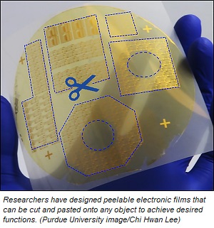
Researchers at Purdue University and the University of Virginia have developed a new fabrication method that makes tiny, thin-film electronic circuits peelable from a surface. The technique not only eliminates several manufacturing steps and the associated costs, but also allows any object to sense its environment or be controlled through the application of a high-tech sticker.
Eventually, these stickers could also facilitate wireless communication. The researchers demonstrate capabilities on various objects in a paper recently published in the Proceedings of the National Academy of Sciences.
"We could customize a sensor, stick it onto a drone, and send the drone to dangerous areas to detect gas leaks, for example," said Chi Hwan Lee, Purdue assistant professor of biomedical engineering and mechanical engineering.
*Most of today’s electronic circuits are individually built on their own silicon “wafer,” a flat and rigid substrate. The silicon wafer can then withstand the high temperatures and chemical etching that are used to remove the circuits from the wafer.
But high temperatures and etching damage the silicon wafer, forcing the manufacturing process to accommodate an entirely new wafer each time.
Lee’s new fabrication technique, called “transfer printing,” cuts down manufacturing costs by using a single wafer to build a nearly infinite number of thin films holding electronic circuits. Instead of high temperatures and chemicals, the film can peel off at room temperature with the energy-saving help of simply water.
“It’s like the red paint on San Francisco’s Golden Gate Bridge – paint peels because the environment is very wet,” Lee said. “So in our case, submerging the wafer and completed circuit in water significantly reduces the mechanical peeling stress and is environmentally friendly.”
A ductile metal layer, such as nickel, inserted between the electronic film and the silicon wafer, makes the peeling possible in water. These thin-film electronics can then be trimmed and pasted onto any surface, granting that object electronic features.
Putting one of the stickers on a flower pot, for example, made that flower pot capable of sensing temperature changes that could affect the plant’s growth.
Lee’s lab also demonstrated that the components of electronic integrated circuits work just as well before and after they were made into a thin film peeled from a silicon wafer. The researchers used one film to turn on and off an LED light display.
“We’ve optimized this process so that we can delaminate electronic films from wafers in a defect-free manner,” Lee said.
A YouTube video is available below:
Share on:


Suggested Items
GlobalFoundries Commits to Achieving Net Zero Emissions and Carbon-Neutral Power by 2050
04/23/2024 | GlobalFoundriesGlobalFoundries (GF) is furthering its commitment to sustainable operations and fighting climate change with the announcement of two new long-term goals to achieve net-zero greenhouse gas (GHG) emissions and 100% carbon-neutral power by 2050.
ROHM Group Company SiCrystal and STMicroelectronics Expand Silicon Carbide Wafer Supply Agreement
04/23/2024 | ROHMROHM and STMicroelectronics, a global semiconductor leader serving customers across the spectrum of electronics applications, announced today the expansion of the existing multi-year, long-term 150mm silicon carbide (SiC) substrate wafers supply agreement with SiCrystal, a ROHM group company.
IDTechEx Report Unveils 3D Electronics Status and Opportunities
04/22/2024 | PRNewswire3D electronics is an emerging manufacturing approach that enables electronics to be integrated within or onto the surface of objects. 3D electronic manufacturing techniques empower new features, including mass customizability, greater integration, and improved sustainability in the electronics industry.
Altus Group Helps BitBox Unlock Productivity and Efficiency Gains with New Reflow Oven
04/22/2024 | Altus GroupAltus Group, a leading provider of capital equipment, has recently assisted BitBox, a UK-based electronics design, engineering and manufacturing company in upgrading its operations with the implementation of a new reflow oven from Heller Industries.
Growth Potential: Electronics Manufacturing Driving Massive Surge in Manufacturing Investment
04/22/2024 | Shawn DuBravac, IPCIn the early months of the pandemic, investment in manufacturing infrastructure, such as plants and production facilities, declined sharply. Real investment dropped over 11%, before finally recovering to pre-pandemic levels in the first half of 2022. Over the past two years, however, several factors have combined to drive manufacturing investment to record levels.