


 Marcy's Musings: The Growing Industry
 It’s Only Common Sense: Here’s What To Do After IPC APEX EXPO 2024
 Dan’s Biz Bookshelf: Seeing the How
Future Electronic Components to Be Printed Like Newspapers
July 20, 2018 | Purdue UniversityEstimated reading time: 2 minutes
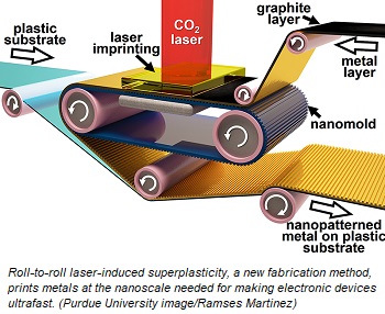
A new manufacturing technique uses a process similar to newspaper printing to form smoother and more flexible metals for making ultra-fast electronic devices.
The low-cost process, developed by Purdue University researchers, combines tools already used in industry for manufacturing metals on a large scale, but uses the speed and precision of roll-to-roll newspaper printing to remove a couple of fabrication barriers in making electronics faster than they are today.
Cellphones, laptops, tablets, and many other electronics rely on their internal metallic circuits to process information at high speed. Current metal fabrication techniques tend to make these circuits by getting a thin rain of liquid metal drops to pass through a stencil mask in the shape of a circuit, kind of like spraying graffiti on walls.
"Unfortunately, this fabrication technique generates metallic circuits with rough surfaces, causing our electronic devices to heat up and drain their batteries faster," said Ramses Martinez, assistant professor of industrial engineering and biomedical engineering.
Future ultrafast devices also will require much smaller metal components, which calls for a higher resolution to make them at these nanoscale sizes.
"Forming metals with increasingly smaller shapes requires molds with higher and higher definition, until you reach the nanoscale size," Martinez said. "Adding the latest advances in nanotechnology requires us to pattern metals in sizes that are even smaller than the grains they are made of. It's like making a sand castle smaller than a grain of sand."
This so-called "formability limit" hampers the ability to manufacture materials with nanoscale resolution at high speed.
Purdue researchers have addressed both of these issues – roughness and low resolution – with a new large-scale fabrication method that enables the forming of smooth metallic circuits at the nanoscale using conventional carbon dioxide lasers, which are already common for industrial cutting and engraving.
"Printing tiny metal components like newspapers makes them much smoother. This allows an electric current to travel better with less risk of overheating," Martinez said.
The fabrication method, called roll-to-roll laser-induced superplasticity, uses a rolling stamp like the ones used to print newspapers at high speed. The technique can induce, for a brief period of time, "superelastic" behavior to different metals by applying high-energy laser shots, which enables the metal to flow into the nanoscale features of the rolling stamp – circumventing the formability limit.
"In the future, the roll-to-roll fabrication of devices using our technique could enable the creation of touch screens covered with nanostructures capable of interacting with light and generating 3D images, as well as the cost-effective fabrication of more sensitive biosensors," Martinez said.
Share on:


Suggested Items
Europlacer Announces Introductory Promotions for 2024 IPC APEX EXPO
03/27/2024 | EuroplacerEuroplacer, a leading provider of SMT assembly solutions, is excited to announce special introductory promotions for its latest products at the upcoming 2024 IPC APEX EXPO, scheduled to take place April 9-11, 2024 at the Anaheim Convention Center in California.
GEN3 to Demo SIR Testing, Stencil Cleaning & More with Horizon Sales at IPC APEX 2024
03/07/2024 | Gen3Gen3, global leader in SIR, CAF, Solderability, Ionic Contamination & process optimisation equipment, to announce its participation in the 2024 IPC APEX EXPO, scheduled to take place April 9-11, 2024 at the Anaheim Convention Center in California. At booth 3934, GEN3 will be exhibiting alongside Horizon Sales, presenting a lineup of advanced technologies aimed at enhancing the efficiency and reliability of circuit assembly processes.
AAT's Patented Rotational Spraying Method Ensures Superior Cleaning Performance
03/07/2024 | Austin American Technology (AAT)Austin American Technology (AAT) is pleased to announce that its patented rotational spraying method ensures superior cleaning performance, delivering consistent results for critical electronic components.
StenTech’s Photo Stencil Specialized Products Division Facility Update Completed
02/27/2024 | StenTechStenTech® Inc., a leading global company specializing in SMT Printing Solutions, has completed a major technology update to their Photo Stencil Specialized Products Division in Golden, Colorado. The phase-one overhaul included upgrades to key areas, including imaging, chemical plating, and chemical coating, along with refreshed offices and board room.
Stencil and PCB Cleaning Solutions from KYZEN at SMTA Monterrey
02/27/2024 | KyzenKYZEN, the global leader in innovative environmentally friendly cleaning chemistries, will exhibit at the SMTA Monterrey Expo & Tech Forum, scheduled to take place Thursday, March 14, 2024 at the Cintermex Convention Center, Hall 2A in Monterrey, Nuevo León. KYZEN will showcase the new aqueous chemistry AQUANOX A4618 in addition to highlighting stencil cleaning chemistries KYZEN E5631J and CYBERSOLV C8882.