


 Marcy's Musings: The Growing Industry
 It’s Only Common Sense: Here’s What To Do After IPC APEX EXPO 2024
 Dan’s Biz Bookshelf: Seeing the How
Diamond Dust Enables Low-Cost, High-Efficiency Magnetic Field Detection
September 12, 2018 | UC BerkeleyEstimated reading time: 3 minutes
UC Berkeley engineers have created a device that dramatically reduces the energy needed to power magnetic field detectors, which could revolutionize how we measure the magnetic fields that flow through our electronics, our planet and even our bodies.
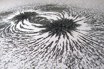
Image Caption: A new device developed by UC Berkeley engineers provides low-cost, high-efficiency magnetic field detection. (Credit: Windell Oskay, via Flickr)
“The best magnetic sensors out there today are bulky, only operate at extreme temperatures and can cost tens of thousands of dollars,” said Dominic Labanowski, who helped create the device, which is made from nitrogen-infused diamonds, as a postdoctoral researcher in the Department of Electrical Engineering and Computer Science. “Our sensors could replace those more-difficult-to-use sensors in a lot of applications from navigation to medical imaging to natural resource exploration.”
Each time a diamond-based sensor measures a magnetic field, it must first be blasted with 1 to 10 watts of microwave radiation to prime them to be sensitive to magnetic fields, which is enough power to melt electronic components. The researchers found a new way to excite tiny diamonds with microwaves using 1,000 times less power, making it feasible to create magnetic-sensing devices that can fit into electronics like cell phones.
This work was led by the lab of EECS professor Sayeef Salahuddin at UC Berkeley in collaboration with researchers from the Ohio State University. The team reports their device online Sep. 7 in the journal Science Advances.
Defective Diamonds
Bombarding a diamond with a jet of nitrogen gas can knock out some of its highly ordered carbon atoms, replacing them with nitrogen atoms. These nitrogen interlopers — called nitrogen vacancy (NV) centers — have unique properties that are well understood by scientists.
“You can use these NV centers as very powerful sensors, but traditionally their applications have been limited because it takes a lot of power to read them,” said Labanowski.
A Greenish Yellow Colored Film with Black Spots
In the device, which is about the size of a fingernail, clusters of diamond nanocrystals (black spots) sit atop a material called a multiferroic. The multiferroic transmits microwave energy into the crystals much more efficiently than other methods.
To detect magnetic fields, scientists first have to hit the NV centers with high-powered microwave radiation, equal to about one-hundredth the power of your standard microwave or 10 times the power consumed by an average cell phone. They then illuminate the NV centers with a laser, which is absorbed and emitted by the nitrogen atoms.
Image Caption: The strength of the magnetic field is related to the strength of the emitted laser light: the intensity of the emitted light can be used to measure the field strength.
To create the device, the researchers placed diamond nanocrystals — containing thousands of NV centers apiece — onto a film called a multiferroic. This new type of material is capable of transferring microwave energy to the crystals much more efficiently.
“This technique dramatically lowers the power consumption of the sensors and makes them usable for realistic applications,” Labanowski said.
Imaging Inside the Body and Under the Earth
Medical applications of magnetic sensors include magnetoencephalography, which uses magnetic fields to measure brain waves, or magnetocardiography, which uses magnetic fields to image heart function. Currently these machines are the size of a small room and can cost upwards of $3 million.
“With low-power NV sensors, you could imagine taking a room-sized magnetoencephalography machine and turning it into something like a helmet, dramatically reducing the size and the costs,” Labanowski said.
The sensors could also be placed in planes or drones to aid in spotting rare earth metals underground, or used in cell phones to improve navigation.
Magnetic field detection is just one application of NV centers, Salahuddin says. The team is planning to refine their technology to use NV centers and other types of quantum systems in a wide variety of applications.
“While we emphasized magnetic field sensing, our work could lead to electrical manipulation of quantum systems in general with much broader areas of application including quantum computing,” Salahuddin said.
Co-authors of the paper are V. Praveen Bhallamudi, Qiaochi Guo, Carola M. Purser and Brendan A. McCullian from the Department of Physics at The Ohio State University.
Share on:


Suggested Items
Inkjet Solder Mask ‘Has Arrived’
04/10/2024 | Pete Starkey, I-Connect007I was delighted to be invited to attend an interactive webinar entitled “Solder Mask Coating Made Easy with Additive Manufacturing,” hosted by SUSS MicroTec Netherlands in Eindhoven. The webinar was introduced and moderated by André Bodegom, managing director at Adeon Technologies, and the speakers were Mariana Van Dam, senior product manager PCB imaging solutions at AGFA in Belgium; Ashley Steers, sales manager at Electra Polymers in the UK; and Dr. Luca Gautero, product manager at SUSS MicroTec Netherlands.
NetVia Group Acquires Direct Imaging from Mivatek
04/09/2024 | Miva TechnologiesMiva Technologies is pleased to announce NetVia Group, Irving, TX has acquired a new Miva 2400NG Dual Tray Direct Imaging System with 30-micron capabilities for inner, outer and soldermask imaging.
Teledyne to Acquire Adimec
02/13/2024 | TeledyneTeledyne Technologies Incorporated announced that it has entered into an agreement to acquire Adimec Holding B.V. and its subsidiaries.
Real Time with... productronica 2023: MivaTek Global Advances Technology With High-res Imaging System
12/08/2023 | Real Time with...productronicaMivaTek's Brendan Hogan talks about how the company employs Digitally Adaptive Rasterization Technology (DART) in their high-res imaging equipment. He also shares how the blurred line between semiconductors and microelectronics is driving broader application of the imaging process.
Keysight Enables Validation of Arbe 4D Imaging Radar Chipset
11/30/2023 | Keysight Technologies, Inc.Keysight Technologies, Inc. announces that Arbe has selected the E8719A Radar Target Solution (RTS) to test the Arbe 4D imaging radar chipset for automotive applications.