


 It’s Only Common Sense: OCCAM—the Time Is Now
 Marcy's Musings: The Growing Industry
 Dan’s Biz Bookshelf: Seeing the How
Shrinking Semiconductor Lasers to the Nanoscale
September 14, 2018 | A*STAREstimated reading time: 2 minutes
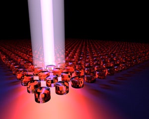
A tiny laser comprising an array of nanoscale semiconductor cylinders (see image) has been made by an all-A*STAR team. This is the first time that lasing has been achieved in non-metallic nanostructures, and it promises to lead to miniature lasers usable in a wide range of optoelectronic devices.
Microscale lasers are widely used in devices such as CD and DVD players. Now, optical engineers are developing nanoscale lasers — so small that they cannot be seen by the human eye.
A promising method is to use arrays of tiny structures made from semiconductors with a high refractive index. Such structures act as tiny antennas, resonating at specific wavelengths. However, it has been challenging to use them to construct a cavity — the heart of a laser, where light bounces around while being amplified.
Now, Arseniy Kuznetsov, Son Tung Ha, Ramón Paniagua-Domínguez, and their colleagues at the A*STAR Institute of Materials Research and Engineering have overcome this problem by exploiting a highly unusual type of standing wave that remains in one spot despite coexisting with a continuous spectrum of radiating waves that can transport energy away. First predicted by quantum mechanics, this wave was demonstrated experimentally in optics about a decade ago.
There was an element of serendipity in the invention. “We initially planned to create a laser just based on the diffractive resonances in the array,” recalls Kuznetsov. “But after fabricating samples and testing them, we discovered this strong enhancement at a different wavelength from expected. When we went back and did further simulations and analysis, we realized that we had created these special waves.”
The demonstration is the culmination of five years of research by the team. It was a race against time, since other groups were also working on developing active nanoantennas, Kuznetsov notes. “Until now, lasing hasn’t been realized in nanoantenna structures,” he says. “So it’s a big step for the dielectric nanoantenna community.”
Their laser also has advantages over other kinds of miniature lasers. Firstly, the direction of its narrow, well-defined beam can be easily controlled — this maneuverability is often needed in device applications. Also, because the nanocylinders are quite sparsely distributed, the laser is highly transparent, which is beneficial for multilayer devices that contain other optical components.
The team is now working to develop lasers that can be excited electrically, rather than by light as in the present study, which would be a major advance toward realizing commercial nanolasers.
Share on:


Suggested Items
IDTechEx Examines the Opportunities for Wearables in Digital Health
04/19/2024 | IDTechExIDTechEx’s report, “Digital Health and Artificial Intelligence 2024-2034: Trends, Opportunities, and Outlook”, covers this ongoing trend in the consumer health wearables market and includes analysis of the opportunities and roadmap for biometric monitoring.
NCAB Appoints Tim Benjamin as New CFO
04/15/2024 | NCAB GroupNCAB Group has appointed Tim Benjamin as its new CFO. Tim has a long and broad experience of managerial business finance roles, including M&A and IT.
Plastronics and the New IPC Guidelines for In-mold Electronics (IME)
04/11/2024 | Barry Matties, I-Connect007In the ever-evolving world of electronics, the roads for the integration of electronics assemblies into 3D structures continue to grow into a set of technologies used to produce 3D plastronics parts and revolutionize mainly the automotive industry. IPC has been developing standards for this set of technologies, led by Francisco Fourcade, IPC electronics technology standards manager.
IEC USA Congratulates Bernie Consitt for 25 Years of Service
04/09/2024 | IECJoin us in celebrating Bernie Consitt's 25 years of service and camaraderie at IEC (International Electronic Components). Bernie has been instrumental in his role as Accounting Manager, helping to supervise, track, and evaluate day-to-day activities within the accounting team.
Helena Maripuu Joins Incap as Group Communication and IR Lead
04/08/2024 | IncapFrom 1 April, communications expert Helena Maripuu joined the headquarters and team of Incap, an international electronics manufacturing services company, to share her long-term experience in the communications and marketing industry and to take the lead in managing processes for Group communication and Investor Relations.