


 Marcy's Musings: The Growing Industry
 It’s Only Common Sense: Here’s What To Do After IPC APEX EXPO 2024
 Dan’s Biz Bookshelf: Seeing the How
New Fabs Invest Over $220 Billion; 2019 to Mark All-Time Spending High
September 18, 2018 | Globe NewswireEstimated reading time: 2 minutes
Global fab equipment spending will increase 14% this year to $62.8 billion and is expected to rise 7.5%, to $67.5 billion, in 2019, marking the fourth consecutive year of spending growth and the highest investment year for fab equipment in the history of the industry, according to the latest World Fab Forecast Report published today by SEMI. Investments in new fab construction are also nearing a record with a fourth consecutive year of growth predicted and capital outlays next year approaching $17 billion.
Investments for fab technology and product upgrades, as well as for additional capacity, will grow as the emergence of numerous new fabs significantly increases equipment demand, the forecast shows. The World Fab Forecast Report currently tracks 78 new fabs and lines that have or will start construction between 2017 to 2020 (with various probabilities) and will eventually require more $220 billion in fab equipment. Construction spending for these fabs and lines is expected to reach $53 billion during this period.
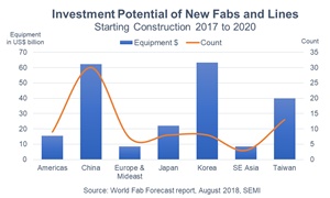
Korea is projected to lead other regions in fab equipment investments with $63 billion, $1 billion more than second-place China. Taiwan is expected to claim the third spot at $40 billon, followed by Japan at $22 billion and the Americas at $15 billion. Europe and Southeast Asia will share sixth place, with investments totaling US$8 billion each. Fully 60% of these fabs will serve the memory sector (the lion’s share will be 3D NAND), and a third will go to foundry.
Of the 78 fab construction projects starting construction between 2017 and 2020, 59 began construction in the first two years (2017 and 2018), while 19 are expected to begin in the last two years (2019 and 2020) of the tracking period.
Equipping a new fab typically takes one to one and a half years, though some fabs take two years and others longer, depending on various factors as such the company, fab size, product type and region. Approximately half of the projected $220 billion will be spent from 2017 and 2020, with less than 10% invested in 2017 and 2018, nearly 40% in 2019 and 2020, and the rest after 2020.
While the $220 billion estimate is based on current insights of known and announced fab plans, total spending could exceed this level as many companies continue to announce plans for new fabs. Since the last quarterly publication of the report published last quarter, 18 new records – all new fabs – have been added to the forecast. Up-to-date and detailed analysis, with a bottoms-up approach, is available by subscribing to SEMI’s World Fab Forecast Report.
Since its June 1 publication, more than 340 updates have been made to the World Fab Forecast. The report now includes more than 1,200 records of current and future front-end semiconductor facilities from high-volume production to research and development. The report covers data and predictions through 2019, including milestones, detailed investments by quarter, product types, technology nodes and capacities down to fab and project level.
About SEMI
SEMI connects over 2,000 member companies and 1.3 million professionals worldwide to advance the technology and business of electronics manufacturing. SEMI members are responsible for the innovations in materials, design, equipment, software, devices, and services that enable smarter, faster, more powerful, and more affordable electronic products. FlexTech, the Fab Owners Alliance (FOA) and the MEMS & Sensors Industry Group (MSIG) are SEMI Strategic Association Partners, defined communities within SEMI focused on specific technologies. Since 1970, SEMI has built connections that have helped its members prosper, create new markets, and address common industry challenges together. SEMI maintains offices in Bangalore, Berlin, Brussels, Grenoble, Hsinchu, Seoul, Shanghai, Silicon Valley (Milpitas, California), Singapore, Tokyo, and Washington, D.C.
Share on:


Suggested Items
KIC’s Miles Moreau to Present Profiling Basics and Best Practices at SMTA Wisconsin Chapter PCBA Profile Workshop
01/25/2024 | KICKIC, a renowned pioneer in thermal process and temperature measurement solutions for electronics manufacturing, announces that Miles Moreau, General Manager, will be a featured speaker at the SMTA Wisconsin Chapter In-Person PCBA Profile Workshop.
The Drive Toward UHDI and Substrates
09/20/2023 | I-Connect007 Editorial TeamPanasonic’s Darren Hitchcock spoke with the I-Connect007 Editorial Team on the complexities of moving toward ultra HDI manufacturing. As we learn in this conversation, the number of shifting constraints relative to traditional PCB fabrication is quite large and can sometimes conflict with each other.
Standard Of Excellence: The Products of the Future
09/19/2023 | Anaya Vardya -- Column: Standard of ExcellenceIn my last column, I discussed cutting-edge innovations in printed circuit board technology, focusing on innovative trends in ultra HDI, embedded passives and components, green PCBs, and advanced substrate materials. This month, I’m following up with the products these new PCB technologies are destined for. Why do we need all these new technologies?
Experience ViTrox's State-of-the-Art Offerings at SMTA Guadalajara 2023 Presented by Sales Channel Partner—SMTo Engineering
09/18/2023 | ViTroxViTrox, which aims to be the world’s most trusted technology company, is excited to announce that our trusted Sales Channel Partner (SCP) in Mexico, SMTo Engineering, S.A. de C.V., will be participating in SMTA Guadalajara Expo & Tech Forum. They will be exhibiting in Booth #911 from the 25th to the 26th of October 2023, at the Expo Guadalajara in Jalisco, Mexico.
Intel Unveils Industry-Leading Glass Substrates to Meet Demand for More Powerful Compute
09/18/2023 | IntelIntel announced one of the industry’s first glass substrates for next-generation advanced packaging, planned for the latter part of this decade.