


 It’s Only Common Sense: OCCAM—the Time Is Now
 Marcy's Musings: The Growing Industry
 Dan’s Biz Bookshelf: Seeing the How
Draw-Your-Own Electrodes Set to Speed up Development of Micro Detection Devices
November 12, 2018 | Imperial College LondonEstimated reading time: 2 minutes
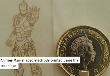
Miniature devices for sensing biological molecules could be developed more quickly thanks to a rapid prototyping method.
Devices that sense and measure biological molecules important for healthcare, such as detecting diseases in blood samples, rely on electrodes to carry out their tasks.
We hope this method will allow bioelectronics to benefit from that ecosystem of hackers getting hands-on with problems and solutions in healthcare.
New generations of these devices are being made that manipulate molecules or work with smaller concentrations of molecules, for example detecting rare cancer cells in blood samples.
These require intricate patterning of minute electrodes. Getting the right pattern is key, but building prototypes of different electrode designs can be expensive and time-consuming, often requiring specialist equipment and expertise.
Now, researchers at Imperial College London, have created a method that allows intricate electrode patterns to be printed in community labs and hackspaces at a fraction of the time and cost. The details of their method are published in Scientific Reports.
Democratising Science
Lead researcher Dr Ali Salehi-Reyhani, from the Department of Chemistry at Imperial, said: “With our method researchers and startups can more easily design and develop analytical devices, even when they need electronics that can’t be bought off-the-shelf.
“Community hackspaces are great for democratising science, allowing more people to try out new technology solutions. We hope this method will allow bioelectronics to benefit from that ecosystem of hackers getting hands-on with problems and solutions in healthcare.”
The method allows researchers to design electrode patterns on computers before printing them off using a laser-cutting printer. The cavities are then filled with metal using microfluidic techniques—using the science of how fluids move through confined spaces.
In this way, researchers could print several sheets of electrodes, each with a slightly different design, allowing them to be tested in rapid succession to find the best design. Previously, designs may have had to be sent away to be manufactured, taking weeks or even months to arrive at the best design, but now the whole process can be reduced to a matter of days.
Manipulating and Analyzing Cells
The team at fabriCELL, a centre of excellence in artificial cell science run by Imperial College London and King’s College London, are now using the technique to prototype devices for manipulating and analysing cells.
They say the technique could be used to speed up the development of flexible wearable devices, such as skin patches that monitor health signals and devices, and devices that could be used in hospitals or GP surgeries, such as ones that can quickly distinguish between viral and bacterial infections with just a drop of blood.
Share on:


Suggested Items
Cadence, TSMC Collaborate on Wide-Ranging Innovations to Transform System and Semiconductor Design
04/25/2024 | Cadence Design SystemsCadence Design Systems, Inc. and TSMC have extended their longstanding collaboration by announcing a broad range of innovative technology advancements to accelerate design, including developments ranging from 3D-IC and advanced process nodes to design IP and photonics.
Ansys, TSMC Enable a Multiphysics Platform for Optics and Photonics, Addressing Needs of AI, HPC Silicon Systems
04/25/2024 | PRNewswireAnsys announced a collaboration with TSMC on multiphysics software for TSMC's Compact Universal Photonic Engines (COUPE). COUPE is a cutting-edge Silicon Photonics (SiPh) integration system and Co-Packaged Optics platform that mitigates coupling loss while significantly accelerating chip-to-chip and machine-to-machine communication.
Siemens’ Breakthrough Veloce CS Transforms Emulation and Prototyping with Three Novel Products
04/24/2024 | Siemens Digital Industries SoftwareSiemens Digital Industries Software launched the Veloce™ CS hardware-assisted verification and validation system. In a first for the EDA (Electronic Design Automation) industry, Veloce CS incorporates hardware emulation, enterprise prototyping and software prototyping and is built on two highly advanced integrated circuits (ICs) – Siemens’ new, purpose-built Crystal accelerator chip for emulation and the AMD Versal™ Premium VP1902 FPGA adaptive SoC (System-on-a-chip) for enterprise and software prototyping.
Listen Up! The Intricacies of PCB Drilling Detailed in New Podcast Episode
04/25/2024 | I-Connect007In episode 5 of the podcast series, On the Line With: Designing for Reality, Nolan Johnson and Matt Stevenson continue down the manufacturing process, this time focusing on the post-lamination drilling process for PCBs. Matt and Nolan delve into the intricacies of the PCB drilling process, highlighting the importance of hole quality, drill parameters, and design optimization to ensure smooth manufacturing. The conversation covers topics such as drill bit sizes, aspect ratios, vias, challenges in drilling, and ways to enhance efficiency in the drilling department.
Elevating PCB Design Engineering With IPC Programs
04/24/2024 | Cory Blaylock, IPCIn a monumental stride for the electronics manufacturing industry, IPC has successfully championed the recognition of the PCB Design Engineer as an official occupation by the U.S. Department of Labor (DOL). This pivotal achievement not only underscores the critical role of PCB design engineers within the technology landscape, but also marks the beginning of a transformative journey toward nurturing a robust, skilled workforce ready to propel our industry into the future.