


 It’s Only Common Sense: OCCAM—the Time Is Now
 Marcy's Musings: The Growing Industry
 Dan’s Biz Bookshelf: Seeing the How
New Materials: Growing Polymer Pelts
November 16, 2018 | KITEstimated reading time: 2 minutes
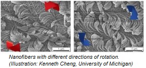
Polymer pelts made of the finest of fibers are suitable for many different applications, from coatings that adhere well and are easy to remove to highly sensitive biological detectors. Researchers at Karlsruhe Institute of Technology (KIT) together with scientists in the United States have now developed a cost-effective process to allow customized polymer nanofibers to grow on a solid substrate through vapor deposition of a liquid crystal layer with reactive molecules.
Surfaces with specially aligned fibers are quite abundant in nature and perform different functions such as sensing, adhering and self-cleaning. For example, the feet of geckos are covered with millions of hairs that allow them to adhere to surfaces and pull off again very easily. The synthesis of such surfaces from man-made materials opens up new perspectives for different applications. However, methods previously available for the production of polymer pelts on solid bases have been costly. What’s more important, the size, shape and alignment of the fibers can only be controlled to a limited extent with conventional methods.
Researchers at the Institute of Functional Interfaces (IFG) of KIT, as well as at the University of Michigan, the University of Wisconsin-Madison and Cornell University in Ithaca, New York, have now developed a simple and therefore cost-effective process that allows polymer pelts to grow in a self-organized way. The research group led by Professor Joerg Lahann, Head of the Department of New Polymers and Biomaterials at KIT’s IFG and Director of the Biointerfaces Institute of the University of Michigan, present the new process in the journal Science. First of all, they cover a carrier with a thin layer of liquid crystals, which are substances that are liquid, have directional properties and are otherwise used especially for screens and displays (liquid crystal displays – LCDs). Next, the liquid crystal layer is exposed to activated molecules by vapor deposition. These reactive monomers penetrate the liquid crystalline layer and grow from the substrate into the liquid in the form of fine fibers.
As a result, polymer nanofibers are created that can be customized in length, diameter, shape and arrangement. The complex but precisely structured polymer pelts formed by the fibers are attractive for many different applications, especially for biological detectors, bioinstructive surfaces that interact with their environment, and for coatings with new properties. This also includes surfaces with dry adhesion properties similar to those of gecko feet, although adhesion in nanofibers is based on a special spatial arrangement of the atoms in the molecules (chirality – handedness).
The German Research Foundation (DFG) funded the work at the “Molecular Structuring of Soft Matter” Collaborative Research Center (CRC). In the 3D Matter Made to Order (3DMM2O) cluster of KIT and the University of Heidelberg, which will be funded in the Excellence Strategy by the federal and state governments from January 2019, the focus will also be on customized materials. The 3DMM2O Excellence Cluster, in which the Head of KIT’s IFG, Professor Christof Wöll, is involved as one of the main researchers, combines natural and engineering sciences, focusing on three-dimensional additive production technologies from a molecular to macroscopic level.
Share on:


Suggested Items
Designer’s Notebook: What Designers Need to Know About Manufacturing, Part 2
04/24/2024 | Vern Solberg -- Column: Designer's NotebookThe printed circuit board (PCB) is the primary base element for providing the interconnect platform for mounting and electrically joining electronic components. When assessing PCB design complexity, first consider the component area and board area ratio. If the surface area for the component interface is restricted, it may justify adopting multilayer or multilayer sequential buildup (SBU) PCB fabrication to enable a more efficient sub-surface circuit interconnect.
Real Time with... IPC APEX EXPO 2024: Advancements in Laser Depaneling with LPKF
04/24/2024 | Real Time with...IPC APEX EXPOJake Benz, LPKF sales manager for North America, discusses the company's advancements in laser depaneling. LPKF has introduced a green wavelength laser for processing rigid FR-4 circuit boards, bringing significant gains in processing speeds to market. The company transitioned from IR CO2 to UV wavelength due to heat and burning issues.
KYZEN to Focus on AQUANOX A4618 at SMTA Wisconsin Expo & Tech Forum
04/22/2024 | KYZEN'KYZEN, the global leader in innovative environmentally friendly cleaning chemistries, will exhibit at the SMTA Wisconsin Expo & Tech Forum, scheduled to take place Tuesday, May 7, 2024 at the Four Poins by Sheraton, Milwaukee Airport in Milwaukee, WI.
AIM Solder’s Dillon Zhu to Present on Ultraminiature Soldering at SMTA China East
04/22/2024 | AIMAIM Solder, a leading global manufacturer of solder assembly materials for the electronics industry, is pleased to announce that Dillon Zhu will present on the topic: Ultraminiature Soldering: Techniques, Technologies, and Standards at SMTA China East. This event is being held at the Shanghai World Expo Exhibition & Convention Center from April 24-25.
Intel Gaudi, Xeon and AI PC Accelerate Meta Llama 3 GenAI Workloads
04/22/2024 | Intel CorporationMeta launched Meta Llama 3, its next-generation large language model (LLM). Effective on launch day, Intel has validated its AI product portfolio for the first Llama 3 8B and 70B models across Intel® Gaudi® accelerators, Intel® Xeon® processors, Intel® Core™ Ultra processors and Intel® Arc™ graphics.