


 It’s Only Common Sense: OCCAM—the Time Is Now
 Marcy's Musings: The Growing Industry
 Dan’s Biz Bookshelf: Seeing the How
Researchers Demonstrate Low Voltage LEDs
August 1, 2019 | University of ManchesterEstimated reading time: 2 minutes
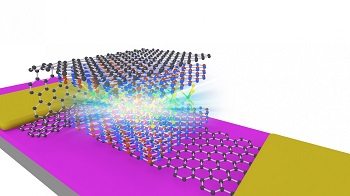
When atomically thin semiconductors are combined together in a Lego style, they emit light at a lower voltage potentially leading to low energy consumption devices.
Whilst this research is in its fundamental state this shows promise for practical applications in optoelectronics and telecommunications.
The voltage of an LED is usually equal to or larger than the bandgap energy per electron charge. A team of researchers based at The University of Manchester, University of Warsaw, the High Magnetic Field Laboratory in Grenoble and the National Institute for Materials Science in Japan have been able to demonstrate LEDs that turn on at much lower voltages.
The idea to stack layers of different materials to make so-called heterostructures goes back to the 1960s, when semiconductor gallium arsenide was researched for making miniature lasers—which are now widely used.
Today, heterostructures are common and are used very broadly in semiconductor industry as a tool to design and control electronic and optical properties in devices.
More recently in the era of atomically thin two-dimensional (2D) crystals, such as graphene, new types of heterostructures have emerged, where atomically thin layers are held together by relatively weak van der Waals forces.
The new structures nicknamed ‘van der Waals heterostructures’ open a huge potential to create numerous designer-materials and novel devices by stacking together any number of atomically thin layers. Hundreds of combinations become possible otherwise inaccessible in traditional three-dimensional materials, potentially giving access to new unexplored optoelectronic device functionality or unusual material properties.
There are a lot of experiments done by various research groups in the world, which focus on light emitting properties of transition metal dichalcogenides. However, often these studies are done purely by optical means. For practical applications, electrically triggered light emission is more desirable.
As published in Nature Communications, the team led by Dr Aleksey Kozikov, Professor Kostya Novoselov and Prof. Marek Potemski were able to do this using electricity. They bound electrons and holes sitting in different transition metal dichalcogenides, so-called interlayer excitons. The researchers created experimental conditions when these excitons recombine non-radiatively, Auger effect. The released energy is transferred to other carriers that can then move to higher energy states. As a result, charge carriers whose energy was originally too low to overcome the material’s bandgap can now easily cross this potential barrier, recombine and emit light. This effect is called upconversion.
Graphene electrodes are used to electrically inject charge carriers through hexagonal boron nitride stacked in a heterostructure into Molybdenum disulphide (MoS2) and Tungsten diselenide (WSe2). Changing the distance between these transition metal dichalcogenides by adding boron nitride in between allows tuning the LEDs from a normal operation to a low-voltage operation and observing the effect of upconversion.
From the fundamental point of view the observed effects mark an important step towards the realisation of exciton condensation and superfluidity of van der Waals heterostructures.
Dr. Johannes Binder, the first author of the paper, from the University of Warsaw said: “When we started measuring the first MoS2/WSe2 devices we were really surprised to observe emission at such low applied voltages. This upconverted emission impressively shows the importance of Auger processes for interlayer excitons in van der Waals heterostructures. Our findings shed more light on the physics in the largely unexplored high carrier density regime, which is crucial for optoelectronic applications as well as for fundamental phenomena like interlayer exciton condensation.”
Dr. Aleksey Kozikov added: “It is fascinating how adding just one atomically thin material can change properties of a device so dramatically. This is the power of van der Waals heterostructures in action”.
Share on:


Suggested Items
Groundbreaking Ceremony Marks the Beginning of a New Era for Newccess Industrial; The Construction of the MINGXIN Building
04/12/2024 | Newccess IndustrialOn a clear and sunny day in March, the groundbreaking ceremony for the MINGXIN Building took place in Shenzhen, China. This moment marked the official commencement of construction for a project that will reshape the semiconductor materials industry.
The Need for a Holistic Global Sustainability Standard
04/10/2024 | Michael Ford, Aegis SoftwareNo one can deny that the resources of our fragile planet are finite. The environment seems like a third party, subject to constant degradation. We’re acutely aware of the effects of pollution on our climate, and despite our “throw-away” culture, recycling and recovery of materials has remained relatively expensive, even as we use more energy just to survive.
iNEMI Publishes Four Roadmap Topics
04/04/2024 | iNEMIThe International Electronics Manufacturing Initiative (iNEMI) announces the availability of the first roadmap topics in the new iNEMI Roadmap format. Printed circuit boards, sustainable electronics, smart manufacturing, and mmWave materials and test are now available online.
Insulectro’s 'Storekeepers' Extend Their Welcome to Technology Village at IPC APEX EXPO
04/03/2024 | InsulectroInsulectro, the largest distributor of materials for use in the manufacture of PCBs and printed electronics, welcomes attendees to its TECHNOLOGY VILLAGE during this year’s IPC APEX EXPO at the Anaheim Convention Center, April 9-11, 2024.
Checking In With ICAPE Group
04/03/2024 | Nolan Johnson, I-Connect007ICAPE Group’s field application engineer Erik Pederson drills down on sustainability, supply chain resiliency, and what value engineering really looks like in this exclusive interview. Founded in 1999, European-based ICAPE Group provides 21 million printed circuit boards and over six million technical parts to manufacturers every month. With 30 PCB manufacturing partners globally and 50 partners providing a wide array of technical parts, ICAPE Group has operations in China, Taiwan, Thailand, South Korea, Vietnam, South Africa, Europe, Mexico, and the United States. The company also focuses on the value proposition for its customers.