


 It’s Only Common Sense: OCCAM—the Time Is Now
 Marcy's Musings: The Growing Industry
 Dan’s Biz Bookshelf: Seeing the How
Graphene Layer Enables Advance in Super-Resolution Microscopy
September 5, 2019 | University of GöttingenEstimated reading time: 1 minute
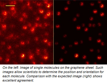
Researchers at the University of Göttingen have developed a new method that takes advantage of the unusual properties of graphene to electromagnetically interact with fluorescing (light-emitting) molecules. This method allows scientists to optically measure extremely small distances, in the order of 1 ångström (one ten-billionth of a meter) with high accuracy and reproducibility for the first time. This enabled researchers to optically measure the thickness of lipid bilayers, the stuff that makes the membranes of all living cells.
Researchers from the University of Göttingen led by Professor Enderlein used a single sheet of graphene, just one atom thick (0.34 nm), to modulate the emission of light-emitting (fluorescent) molecules when they came close to the graphene sheet. The excellent optical transparency of graphene and its capability to modulate through space the molecules’ emission made it an extremely sensitive tool for measuring the distance of single molecules from the graphene sheet. The accuracy of this method is so good that even the slightest distance changes of around 1 ångström (this is about the diameter of an atom or half a millionth of a human hair) can be resolved.
The scientists were able to show this by depositing single molecules above a graphene layer. They could then determine their distance by monitoring and evaluating their light emission. This graphene-induced modulation of molecular light emission provides an extremely sensitive and precise “ruler” for determining single molecule positions in space. They used this method to measure the thickness of single lipid bilayers which are constituted of two layers of fatty acid chain molecules and have a total thickness of only a few nanometers (1 billionth of a meter).
“Our method has enormous potential for super-resolution microscopy because it allows us to localise single molecules with nanometre resolution not only laterally (as with earlier methods) but also with similar accuracy along the third direction, which enables true three-dimensional optical imaging on the length scale of macromolecules,” says Arindam Ghosh, the first author of the paper.
“This will be a powerful tool with numerous applications to resolve distances with sub-nanometer accuracy in individual molecules, molecular complexes, or small cellular organelles,” adds Professor Jörg Enderlein, the publication’s corresponding author and head of the Third Institute of Physics (Biophysics) where the work took place.
Share on:


Suggested Items
Inkjet Solder Mask ‘Has Arrived’
04/10/2024 | Pete Starkey, I-Connect007I was delighted to be invited to attend an interactive webinar entitled “Solder Mask Coating Made Easy with Additive Manufacturing,” hosted by SUSS MicroTec Netherlands in Eindhoven. The webinar was introduced and moderated by André Bodegom, managing director at Adeon Technologies, and the speakers were Mariana Van Dam, senior product manager PCB imaging solutions at AGFA in Belgium; Ashley Steers, sales manager at Electra Polymers in the UK; and Dr. Luca Gautero, product manager at SUSS MicroTec Netherlands.
NetVia Group Acquires Direct Imaging from Mivatek
04/09/2024 | Miva TechnologiesMiva Technologies is pleased to announce NetVia Group, Irving, TX has acquired a new Miva 2400NG Dual Tray Direct Imaging System with 30-micron capabilities for inner, outer and soldermask imaging.
Teledyne to Acquire Adimec
02/13/2024 | TeledyneTeledyne Technologies Incorporated announced that it has entered into an agreement to acquire Adimec Holding B.V. and its subsidiaries.
Real Time with... productronica 2023: MivaTek Global Advances Technology With High-res Imaging System
12/08/2023 | Real Time with...productronicaMivaTek's Brendan Hogan talks about how the company employs Digitally Adaptive Rasterization Technology (DART) in their high-res imaging equipment. He also shares how the blurred line between semiconductors and microelectronics is driving broader application of the imaging process.
Keysight Enables Validation of Arbe 4D Imaging Radar Chipset
11/30/2023 | Keysight Technologies, Inc.Keysight Technologies, Inc. announces that Arbe has selected the E8719A Radar Target Solution (RTS) to test the Arbe 4D imaging radar chipset for automotive applications.