


 It’s Only Common Sense: OCCAM—the Time Is Now
 Marcy's Musings: The Growing Industry
 Dan’s Biz Bookshelf: Seeing the How
Taking 2D Materials to the MAX
October 17, 2019 | KAUSTEstimated reading time: 3 minutes
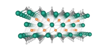
A class of atomically thin 2D compounds, known as MXenes, have a unique combination of properties that are useful for electronic and sensing applications.
Discovered by researchers at Drexel University as electrodes for energy applications, MXenes have become a research focus for KAUST. Husam Alshareef and his team specialize in creating nanomaterials for electronic and energy applications. They turn them into devices, such as supercapacitors, batteries and sensors. The chemically active surface and highly conducting core of MXenes make them an ideal candidate material for the group’s cutting-edge materials research.
MXene membranes, like these fabricated in Alshareef's lab, are used for energy storage, sensing and osmotic power generation.
MXenes typically consist of a core of titanium and carbon atoms, just a few atoms thick. This metallic material (a carbide or nitride) has electrical conductivity comparable to a copper wire. The upper and lower surface of the MXene is covered with metal-oxygen (e.g. Ti-O) and metal-hydroxyl (e.g. Ti-OH) bonds, which are chemically and electrochemically active. “This combination of properties makes MXenes unique,” Alshareef explains.
“Researchers at KAUST have made groundbreaking contributions to applications of MXenes in electronic devices and sensors,” says Yury Gogotsi, a professor from Drexel University in the United States, one of the discoverers of MXenes. “They have moved them from the material stage to the device stage thanks to their experience with electronics. This is very important and may be a defining moment in the practical implementation of MXenes in industry.”
MXenes can be used to create better sensors, touch screens, photodetectors and composites.
Page 1 of 2
Share on:


Suggested Items
Designer’s Notebook: What Designers Need to Know About Manufacturing, Part 2
04/24/2024 | Vern Solberg -- Column: Designer's NotebookThe printed circuit board (PCB) is the primary base element for providing the interconnect platform for mounting and electrically joining electronic components. When assessing PCB design complexity, first consider the component area and board area ratio. If the surface area for the component interface is restricted, it may justify adopting multilayer or multilayer sequential buildup (SBU) PCB fabrication to enable a more efficient sub-surface circuit interconnect.
Insulectro’s 'Storekeepers' Extend Their Welcome to Technology Village at IPC APEX EXPO
04/03/2024 | InsulectroInsulectro, the largest distributor of materials for use in the manufacture of PCBs and printed electronics, welcomes attendees to its TECHNOLOGY VILLAGE during this year’s IPC APEX EXPO at the Anaheim Convention Center, April 9-11, 2024.
ENNOVI Introduces a New Flexible Circuit Production Process for Low Voltage Connectivity in EV Battery Cell Contacting Systems
04/03/2024 | PRNewswireENNOVI, a mobility electrification solutions partner, introduces a more advanced and sustainable way of producing flexible circuits for low voltage signals in electric vehicle (EV) battery cell contacting systems.
Heavy Copper PCBs: Bridging the Gap Between Design and Fabrication, Part 1
04/01/2024 | Yash Sutariya, Saturn Electronics ServicesThey call me Sparky. This is due to my talent for getting shocked by a variety of voltages and because I cannot seem to keep my hands out of power control cabinets. While I do not have the time to throw the knife switch to the off position, that doesn’t stop me from sticking screwdrivers into the fuse boxes. In all honesty, I’m lucky to be alive. Fortunately, I also have a talent for building high-voltage heavy copper circuit boards. Since this is where I spend most of my time, I can guide you through some potential design for manufacturability (DFM) hazards you may encounter with heavy copper design.
Trouble in Your Tank: Supporting IC Substrates and Advanced Packaging, Part 5
03/19/2024 | Michael Carano -- Column: Trouble in Your TankDirect metallization systems based on conductive graphite or carbon dispersion are quickly gaining acceptance worldwide. Indeed, the environmental and productivity gains one can achieve with these processes are outstanding. In today’s highly competitive and litigious environment, direct metallization reduces costs associated with compliance, waste treatment, and legal issues related to chemical exposure. What makes these processes leaders in the direct metallization space?