


 It’s Only Common Sense: OCCAM—the Time Is Now
 Marcy's Musings: The Growing Industry
 Dan’s Biz Bookshelf: Seeing the How
Space Saving, 3.3V I/O FBGA Two-Speed Synchro/Resolver Combiner from DDC
November 22, 2019 | Data Device Corporation (DDC)Estimated reading time: 1 minute
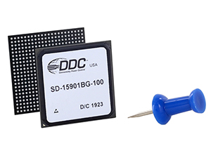
Data Device Corporation (DDC) introduces a redesigned version of its popular Synchro/Resolver two-speed combiner, now featuring 3.3V I/O within a compact and highly efficient FBGA (Fine Pitch Ball Grid Array) package. The SD-15901 FBGA design provides space and power savings with a 34% smaller footprint and 35% less power dissipation than the previous generation, enabling SWaP optimization of PCB layout and ease of assembly with ball grid array surface mounting.
Using coarse and fine digital angle inputs, the combiner provides up to 22-bit angle resolution, making it ideal for high-performance position control systems requiring real-time precision resolution. Additionally, the SD-15901 is RoHS compliant, and rated for the full military temperature range (-55°C to +125°C).
Benefits include:
- Optimized Performance and Design
- High resolution (up to 22 bits)
- Small footprint (23 mm x 23 mm) saves board space, 34% smaller compared with (28.4 mm x 28.4 mm) of previous generation
- Low power dissipation, 35% less power dissipated than previous generation (at nominal operation)
- FBGA design enables ease of assembly
- Flexibility & Ease of Use
- Can be used with all 3.3V Synchro/Resolver converters and processors, no logic shifters required
- No software or calibration required
- Environmental
- Military temperature range (-55°C to +125°C)
- RoHS compliant
"DDC’s second generation Synchro/Resolver two-speed combiner offers significant SWaP savings along with high resolution, to enable optimized PDB design," Roger Tomassi, DDC Product Line Manager, Motion Feedback.
Share on:


Suggested Items
Cadence, TSMC Collaborate on Wide-Ranging Innovations to Transform System and Semiconductor Design
04/25/2024 | Cadence Design SystemsCadence Design Systems, Inc. and TSMC have extended their longstanding collaboration by announcing a broad range of innovative technology advancements to accelerate design, including developments ranging from 3D-IC and advanced process nodes to design IP and photonics.
Ansys, TSMC Enable a Multiphysics Platform for Optics and Photonics, Addressing Needs of AI, HPC Silicon Systems
04/25/2024 | PRNewswireAnsys announced a collaboration with TSMC on multiphysics software for TSMC's Compact Universal Photonic Engines (COUPE). COUPE is a cutting-edge Silicon Photonics (SiPh) integration system and Co-Packaged Optics platform that mitigates coupling loss while significantly accelerating chip-to-chip and machine-to-machine communication.
Siemens’ Breakthrough Veloce CS Transforms Emulation and Prototyping with Three Novel Products
04/24/2024 | Siemens Digital Industries SoftwareSiemens Digital Industries Software launched the Veloce™ CS hardware-assisted verification and validation system. In a first for the EDA (Electronic Design Automation) industry, Veloce CS incorporates hardware emulation, enterprise prototyping and software prototyping and is built on two highly advanced integrated circuits (ICs) – Siemens’ new, purpose-built Crystal accelerator chip for emulation and the AMD Versal™ Premium VP1902 FPGA adaptive SoC (System-on-a-chip) for enterprise and software prototyping.
Elevating PCB Design Engineering With IPC Programs
04/24/2024 | Cory Blaylock, IPCIn a monumental stride for the electronics manufacturing industry, IPC has successfully championed the recognition of the PCB Design Engineer as an official occupation by the U.S. Department of Labor (DOL). This pivotal achievement not only underscores the critical role of PCB design engineers within the technology landscape, but also marks the beginning of a transformative journey toward nurturing a robust, skilled workforce ready to propel our industry into the future.
IPC Design Competition Champion Crowned at IPC APEX EXPO 2024
04/24/2024 | IPCAt IPC APEX EXPO 2024 in Anaheim, California, five competitors squared off to determine who was the best of the best at PCB design.