


 Flexible Thinking: PCB Designers Still Wanted
 Connect the Dots: Five Best Practices for Designing Flex and Rigid-flex PCBs
 Tim’s Takeaways: Human Ingenuity and the Rigid-flex PCB
Decreasing Bend Radius and Improving Reliability- Part III
December 18, 2019 | Kelsey Smith, All FlexEstimated reading time: 1 minute
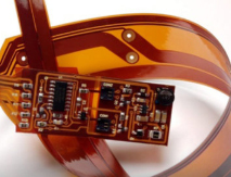
Application: Design guidelines to improve the flexibility and reliability of flexible circuits.
Most issues that arise with flex circuits can be eliminated in the early stages of the design phase, and special planning must occur when the circuit is required to bend. Many novices will design a circuit that calls for bending the flex in too tight of a bend radius, which can cause damage to the circuit and lower the reliability of the end product. This is the third and final installment in a series of articles that will focus on the seven key aspects to consider when designing for maximum durability and maximum “flexibility." It is important to know that because flexibility is a relative term this study will instead use the term reducing bend radius. Below are three of the seven design strategies, please see Part I and Part II for more tips!
5. Apply strain relief at transition areas from stiffener to flex.
- Stiffener material is common in flex circuit designs that have soldered components. While this rigid material is necessary for the soldered components, it can cause reliability issues during installation when the flex is bent at the stiffener location toward the stiffener.
- If the flex material will be bending toward the stiffener, it is highly recommended that an epoxy bead of Ecobond 45 be applied.
6. Ensure vias are located at least .050” away from bend zones.

Fig. 1 - Examples of a flex circuit with a bend radius and a plated through-hole.
7. Always put a 3D representation of your bend to install configuration on your drawings.
- Many problems can be avoided by informing your flex circuit vendor what the final configuration is going to be once used, this enables them to evaluate for potential bend radius issues.
- Most flex circuit drawings are only 2D. By showing a picture of the final configuration you are encouraging the discussion regarding materials, discussion about minimum bend radius and letting the flex vendor raise any concerns before build.

Fig. 2 - Examples of a 3D drawing of a flex circuit.
Share on:


Suggested Items
iNEMI Packaging Tech Topic Series: Role of EDA in Advanced Semiconductor Packaging
04/26/2024 | iNEMIAdvanced semiconductor packaging with heterogenous integration has made on-package integration of multiple chips a crucial part of finding alternatives to transistor scaling. Historically, EDA tools for front-end and back-end design have evolved separately; however, design complexity and the increased number of die-to-die or die-to-substrate interconnections has led to the need for EDA tools that can support integration of overall design planning, implementation, and system analysis in a single cockpit.
Cadence, TSMC Collaborate on Wide-Ranging Innovations to Transform System and Semiconductor Design
04/25/2024 | Cadence Design SystemsCadence Design Systems, Inc. and TSMC have extended their longstanding collaboration by announcing a broad range of innovative technology advancements to accelerate design, including developments ranging from 3D-IC and advanced process nodes to design IP and photonics.
Ansys, TSMC Enable a Multiphysics Platform for Optics and Photonics, Addressing Needs of AI, HPC Silicon Systems
04/25/2024 | PRNewswireAnsys announced a collaboration with TSMC on multiphysics software for TSMC's Compact Universal Photonic Engines (COUPE). COUPE is a cutting-edge Silicon Photonics (SiPh) integration system and Co-Packaged Optics platform that mitigates coupling loss while significantly accelerating chip-to-chip and machine-to-machine communication.
Siemens’ Breakthrough Veloce CS Transforms Emulation and Prototyping with Three Novel Products
04/24/2024 | Siemens Digital Industries SoftwareSiemens Digital Industries Software launched the Veloce™ CS hardware-assisted verification and validation system. In a first for the EDA (Electronic Design Automation) industry, Veloce CS incorporates hardware emulation, enterprise prototyping and software prototyping and is built on two highly advanced integrated circuits (ICs) – Siemens’ new, purpose-built Crystal accelerator chip for emulation and the AMD Versal™ Premium VP1902 FPGA adaptive SoC (System-on-a-chip) for enterprise and software prototyping.
Listen Up! The Intricacies of PCB Drilling Detailed in New Podcast Episode
04/25/2024 | I-Connect007In episode 5 of the podcast series, On the Line With: Designing for Reality, Nolan Johnson and Matt Stevenson continue down the manufacturing process, this time focusing on the post-lamination drilling process for PCBs. Matt and Nolan delve into the intricacies of the PCB drilling process, highlighting the importance of hole quality, drill parameters, and design optimization to ensure smooth manufacturing. The conversation covers topics such as drill bit sizes, aspect ratios, vias, challenges in drilling, and ways to enhance efficiency in the drilling department.