-

- News
- Books
Featured Books
- pcb007 Magazine
Latest Issues
Current Issue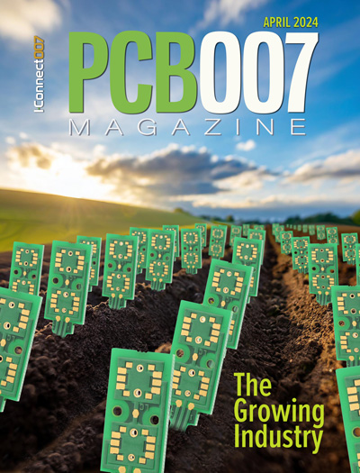
The Growing Industry
In this issue of PCB007 Magazine, we talk with leading economic experts, advocacy specialists in Washington, D.C., and PCB company leadership to get a well-rounded picture of what’s happening in the industry today. Don’t miss it.

The Sustainability Issue
Sustainability is one of the most widely used terms in business today, especially for electronics and manufacturing but what does it mean to you? We explore the environmental, business, and economic impacts.

The Fabricator’s Guide to IPC APEX EXPO
This issue previews many of the important events taking place at this year's show and highlights some changes and opportunities. So, buckle up. We are counting down to IPC APEX EXPO 2024.
- Articles
- Columns
Search Console
- Links
- Events
||| MENU - pcb007 Magazine
AT&S: Working With Designers on a Global Level
February 5, 2020 | Barry Matties, I-Connect007Estimated reading time: 16 minutes
Barry Matties recently took a tour of AT&S’s Austrian factory, which is developing new circuit design strategies surrounding embedded and active components. Gerald Weis discusses the company’s focus on serving and educating PCB designers around the world, as well as their plans to embrace the latest technology and Industry 4.0 processes going forward.
Barry Matties: AT&S has a long history as a leader on many levels. What is your current revenue?
Gerald Weis: We’re proud that we hit $1 billion in the last financial year. At the moment, about 10,000 employees work for our company. What’s interesting is that people are working an average of five to seven years within AT&S, which is longer compared to the industry average. Especially if you look to China, that’s really good.
Barry Matties: Because every Chinese New Year, you tend to lose people. Is your facility in Shanghai?
Weis: Our headquarters is in Leoben, and we have a production site in Fehring; those are all plants in Austria. In Nanjangud, India, we run standard multilayer PCB constructions. Chongqing essentially focuses on substrates; we do small PCBs and substrates there. We do HDI build-ups at AT&S Shanghai, and Ansan is one of our smallest plants, which is responsible for flex PCBs.
Matties: Do you do a lot of flex?
Weis: Yes. We do rigid-flex, full flex, and flex to install, where we use prepreg instead of polyimides. It is bendable for about five or 10 times. Customers usually use it for installing purposes in their fixture.
Matties: How long have you had the facility in India?
Weis: In 1999, we acquired Indal Electronics Ltd., the largest Indian PCB plant in Nanjangud.
Matties: Is there some advantage to the location of your headquarters?
Weis: Based on Austrian economical history, this area around Leoben largely focused on the steel industry. A big iron ore mine was largely exploited, so there are hardly any resources left. In the early ‘80s, the government realized that the steel industry should not be their only focus, so they decided to invest in other industries; they came to the electronics industry to offer jobs for the region. With that, the first plant was built, doing PCBs for IBM. About 25 years ago, AT&S became a privately owned company. The company’s success also came from management decisions.
Matties: When it was privatized, how big was the company?
Weis: At the time, we only had three locations in Austria. There were about 1,500 people overall, which meant €70 million turnover per year.
We have had immense growth over the past 25 years. And our growth is also connected to the success of handheld devices in the early days; that was a big driver.
Matties: Nokia and Research in Motion were big in Europe.
Weis: We have played a major role in the success of these two companies. Last year, I was in the U.S. at the IMAPS Device Packaging Conference, and I recognized that Nokia and its outstanding supply chain is still in developers minds. Nokia has somehow driven the electronics industry in many production-related areas, especially in miniaturization.
Matties: When you say the supply chain, describe what you think it should look like now.
Weis: Embedding of components inside a PCB requires a special surface finishing on the electrically conductive connections. The wafer manufacturer or a third-party supplier usually applies it directly on the wafer. The traceability plays a big role, as the whole supply chain needs to be adapted accordingly. We, as a PCB manufacturer with the ability to embed components inside the PCB, also need to ensure that a reliable interface to the wafer fab is established. It is also essential to trace which silicon die is assembled in which card. To ensure an efficient throughout, you need to understand the whole value chain. A focus on your specific item only is not enough. That’s why we always look at what’s happening one step before and one step after our part in the value chain.
Matties: I would even go further and say you have to look at the first and last step and understand every other step because they’re all connected.
Weis: By wafer manufacturing, you get a wafer and a wafer map indicating all good dies. There is surface finishing, which may be aluminum, but aluminum cannot be connected to copper in a reliable manner. How do you ensure an electrical connection? Usually, you use a redistribution layer to connect the aluminum or gold chip pad to a copper surface, which we can connect directly to the PCB structure. To apply such structure, a wafer manufacturer, a third party, or an in-house process are possible. Those are the scenarios we are thinking of, and that is where we try to get the work done as quickly as possible. Sure, a third party could be the fastest, but it’s also the most expensive way to get it done. In the end, you have to decide based on the project and the layout of the chip as well as the PCB. Typically, we wants to have the fastest and cheapest way, but some compromises need to be taken into account. Additionally, we think about the assembly, as we are able to do direct wafer assembly as well as assembly from tape and reel.
Matties: Are you talking about high-current applications?
Weis: We are not only talking about converters, inverters, and voltages up to 1,200 volts that are needed for lithium-ion batteries. Now, the automotive requirement is 48 volts for the high-power board net. There is a change from 12 volts to 48 volts for start-stop systems and auxiliaries like electric climate control, electric power steering, and more. We also work in the segment of Industry 4.0 and machine-to-machine communication. The industrial sector is more or less concerned about high-performance computing, which involves impedance controlled transmission lines, small line and space requirements, less copper heights, and high layer count. For automotive, the focus is more on high copper weights and large areas to get rid of the heat while a high current throughput is needed.
Matties: Do you see any trends in those areas right now?
Weis: In general, we see automotive as a challenging area. From a European perspective, with the automotive industry being difficult, the whole industrial area is not the easiest one to be in either, but everyone has to cope with that situation. We still benefit because cars are becoming more and more digital, and we are playing in this field. Medical is doing well, and another driver is the mobile device substrates market. Hearing aids, for example, are small. Embedding help to find novel solutions to pursue further miniaturization, enlarge the battery, and extend the overall lifetime. That is an interesting sector for us as well.
Matties: What’s your role here, and what does a typical day look like?
Weis: My role involves hardware development. I work together with customers to optimize actual solutions, develop new ideas, and miniaturize PCBs. I also help to establish new technologies at the customer’s side. My daily bread is to do designs and electrical simulations. For simulations requiring multi-physic approaches, I do those with our in-house simulation department. Together, we try to indicate warpage issues before production. First, we calculate the build-ups, and then we simulate it to ensure proper behavior. If we agree with the results, the production starts.
Matties: And more and more simulations come into play.
Weis: Electrical simulation only is often not enough. Thermal considerations are also interesting, especially for converter and inverter applications. For example, if you have a transistor embedded inside a PCB, you might need some simulation to figure out thermal resistance and compare standard packed devices in terms of performance. Therefore, we have various flexible software packages and experts to ensure fast and reliable simulations, figuring out the results of electric and thermal characteristics. For electrical ones, we focus on H-field, B-field, E-field, and S-parameters for RF-applications. In principle, we simulate solutions for high-performance switching as well as high-frequency transmission.
Matties: But the simulation is only as good as the variables that you input.
Weis: I fully agree. Before starting a simulation, we characterize the behavior of the base materials used. We know exactly how the base material performs. At the front-end simulation of PCB constructions, including plating ensures good results after production. Usually, we do more than one simulation, as there might be some uncertainties after a first run. We also need to consider a production tolerance depending on the layout of the PCB and the material used. In addition, the machine park places a big role.
Matties: What about thermal simulation?
Page 1 of 2
Suggested Items
AIM Solder’s Dillon Zhu to Present on Ultraminiature Soldering at SMTA China East
04/22/2024 | AIMAIM Solder, a leading global manufacturer of solder assembly materials for the electronics industry, is pleased to announce that Dillon Zhu will present on the topic: Ultraminiature Soldering: Techniques, Technologies, and Standards at SMTA China East. This event is being held at the Shanghai World Expo Exhibition & Convention Center from April 24-25.
AIM to Highlight NC259FPA Ultrafine No Clean Solder Paste at SMTA Wisconsin Expo & Tech Forum
04/18/2024 | AIMAIM Solder, a leading global manufacturer of solder assembly materials for the electronics industry, is pleased to announce its participation in the upcoming SMTA Wisconsin Expo & Tech Forum taking place on May 7 at the Four Points by Sheraton | Milwaukee Airport, in Milwaukee, Wisconsin.
Hentec/RPS Publishes an Essential Guide to Selective Soldering Processing Tech Paper
04/17/2024 | Hentec Industries/RPS AutomationHentec Industries/RPS Automation, a leading manufacturer of selective soldering, lead tinning and solderability test equipment, announces that it has published a technical paper describing the critical process parameters that need to be optimized to ensure optimal results and guarantee the utmost in end-product quality.
Empowering Electronics Assembly: Introducing ALPHA Innolot MXE Alloy
04/16/2024 | MacDermid Alpha Electronics SolutionsIn the rapidly evolving electronics industry, where innovation drives progress, MacDermid Alpha Electronics Solutions is committed to setting a new standard. Today, we are pleased to introduce ALPHA Innolot MXE, a revolutionary alloy meticulously engineered to address the critical needs of enhanced reliability and performance in modern electronic assemblies.
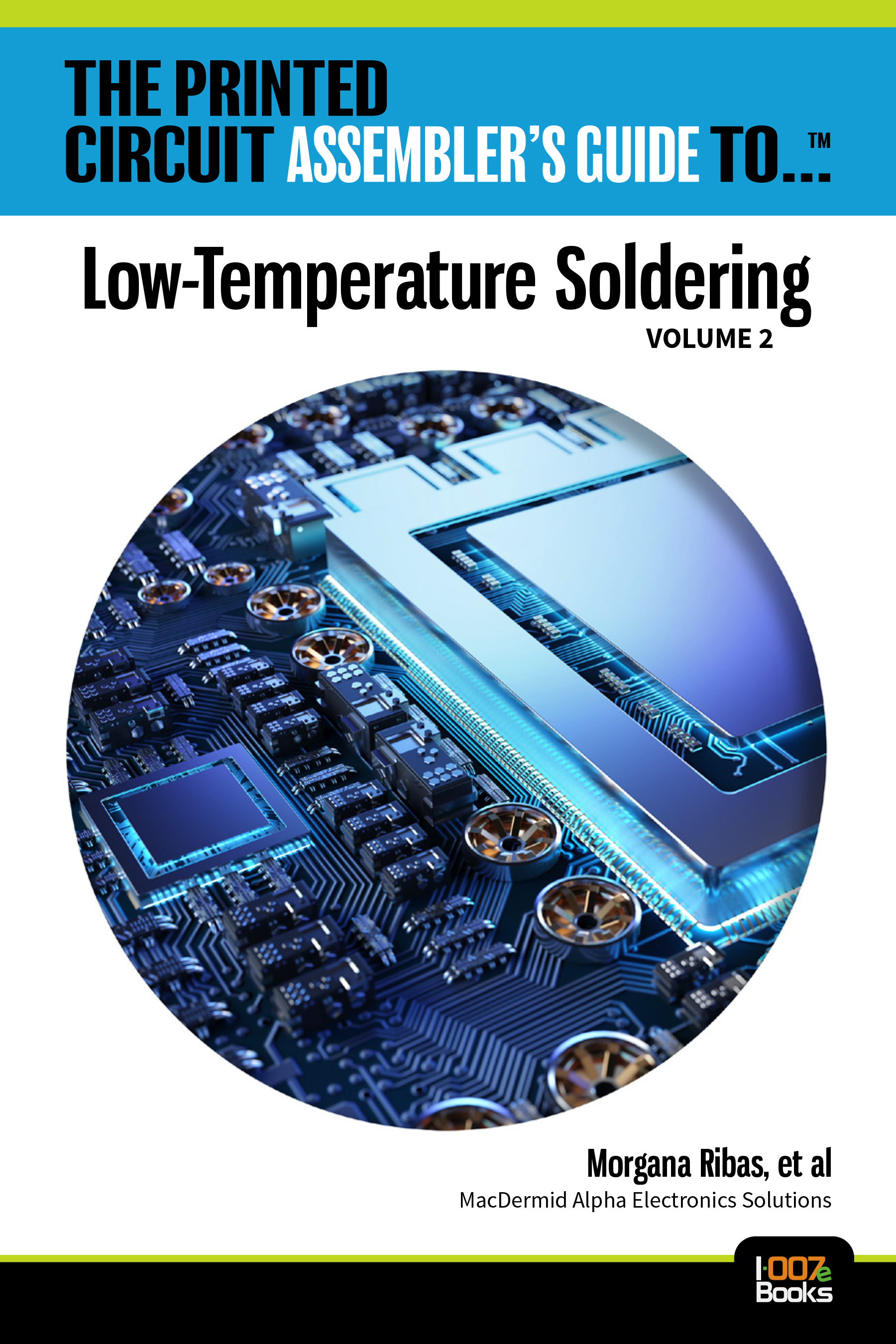
New Book on Low-temperature Soldering Now Available
04/17/2024 | I-Connect007I-Connect007 is pleased to announce that The Printed Circuit Assembler’s Guide to… Low-temperature Soldering, Vol. 2, by subject matter experts at MacDermid Alpha Electronics Solutions, is now available for download.
