


 Marcy's Musings: The Growing Industry
 It’s Only Common Sense: Here’s What To Do After IPC APEX EXPO 2024
 Dan’s Biz Bookshelf: Seeing the How
Limata’s Innovative LUVIR Technology Speeds Up PCB Solder Mask Production
August 6, 2020 | LimataEstimated reading time: 3 minutes
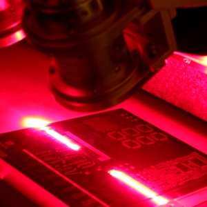
Limata, a provider of Laser Direct Imaging (LDI) systems for PCB manufacturing and adjacent markets, announces the availability of its proprietary and field-proven LUVIR Technology® on all X-series model types. This unique LDI technology significantly increases the speed of solder mask (SM) direct imaging at lower Total Cost of Ownership (TCO).
Innovation reduces required UV-power and increases imaging speed
Direct imaging (DI) of solder masks in PCB manufacturing, which is essential to comply with the latest PCB design requirements in the area of registration and accuracy, has always been a challenging task. Since solder mask inks require significantly higher doses of ultra-violet (UV) energy than dry-film, the imaging processing times of multi-wavelength DI solutions (solely relying on UV-light sources) are either too slow for high-volume requirements or fail to deliver the required SM imaging output capacity at a reasonable investment for the manufacturer.
To tackle this challenge, Limata has developed a completely new approach for solder mask exposure, that utilizes both, UV- and infrared (IR-) lasers. This combined laser approach shortens imaging cycle times and increases throughput (prints or panels per hour) further delivering best-in-class ionic contamination (‘bleeding’) values on all conventional ink types.
"With LUVIR, we are able to deliver the same imaging results at lower UV-laser energy levels of just 100 to 250mJ/cm2 compared with 400 to 1,000mJ/cm2 required on LED/DMD systems – with no compromises on surface quality, resolution or accuracy," said Matthias Nagel, CTO of Limata. "Using IR enables us to downsize the UV-laser capacity in our systems, which supports lower equipment costs, ultimately delivering the best price/performance value of any DI solder mask system currently available in the market.”
Outstanding imaging results on all conventional ink types
Higher imaging efficiency and throughput levels with LUVIR are particularly achieved on all conventional solder mask ink types and colors (green, blue and black) as well as on legend inks (white), further eliminating the need for PCB manufacturers to transition from conventional standard ink material to more expensive DI inks, a change which normally requires lengthy and costly re-certifications of solder mask processes by end-customers or PCB designers. In addition, LUVIR fully supports the digital imaging of PCB structures at coating thicknesses in the 4 mil (100 µm) to 6 mil (150 µm) range without significant undercut. This is a direct imaging task that cannot be processed by multi-wavelength DMD/LED systems at reasonable speed levels or yields.
Lower Cost-per-Print and Total Costs of Ownership for PCB manufacturers
PCB production data from the field have proven a significant imaging and throughput advantage with LUVIR on all conventional solder mask inks at up to 40% lower costs per print compared to DI system peers. The use of long-lifetime components for its UV/IR imaging module complemented by an in-house developed sensor array for the automatic remote calibration of lasers significantly reduces maintenance requirements and after-sales costs by further eliminating the need for manufacturers to enter into expensive long-term service agreements over the equipment lifecycle.
LIMATA’s X2000-series platform, powered by LUVIR in a four UV/IR imaging head configuration, supports high-volume PCB capacity requirements. The availability of LUVIR on a more compact system platform (X1000) lowers the entry barriers for quick-turn-around manufacturers considering transitioning from mask/film and investing in a digital system solution for solder mask direct imaging.
LIMATA was recently acknowledged for its LUVIR innovation with the Productronica Innovation Award 2019 in the PCB & EMS Cluster. The technology is available on all LIMATA X-series system models featuring a range of options addressing individual PCB customer needs in different markets and regions. All X-Series systems also support the direct-imaging of dry-film (photoresist) down to a resolution of 1 mil (25 µm) line and space.
Share on:


Suggested Items
AIM to Highlight NC259FPA Ultrafine No Clean Solder Paste at SMTA Wisconsin Expo & Tech Forum
04/18/2024 | AIMAIM Solder, a leading global manufacturer of solder assembly materials for the electronics industry, is pleased to announce its participation in the upcoming SMTA Wisconsin Expo & Tech Forum taking place on May 7 at the Four Points by Sheraton | Milwaukee Airport, in Milwaukee, Wisconsin.
Hentec/RPS Publishes an Essential Guide to Selective Soldering Processing Tech Paper
04/17/2024 | Hentec Industries/RPS AutomationHentec Industries/RPS Automation, a leading manufacturer of selective soldering, lead tinning and solderability test equipment, announces that it has published a technical paper describing the critical process parameters that need to be optimized to ensure optimal results and guarantee the utmost in end-product quality.
Empowering Electronics Assembly: Introducing ALPHA Innolot MXE Alloy
04/16/2024 | MacDermid Alpha Electronics SolutionsIn the rapidly evolving electronics industry, where innovation drives progress, MacDermid Alpha Electronics Solutions is committed to setting a new standard. Today, we are pleased to introduce ALPHA Innolot MXE, a revolutionary alloy meticulously engineered to address the critical needs of enhanced reliability and performance in modern electronic assemblies.
New Book on Low-temperature Soldering Now Available
04/17/2024 | I-Connect007I-Connect007 is pleased to announce that The Printed Circuit Assembler’s Guide to… Low-temperature Soldering, Vol. 2, by subject matter experts at MacDermid Alpha Electronics Solutions, is now available for download.
Inkjet Solder Mask ‘Has Arrived’
04/10/2024 | Pete Starkey, I-Connect007I was delighted to be invited to attend an interactive webinar entitled “Solder Mask Coating Made Easy with Additive Manufacturing,” hosted by SUSS MicroTec Netherlands in Eindhoven. The webinar was introduced and moderated by André Bodegom, managing director at Adeon Technologies, and the speakers were Mariana Van Dam, senior product manager PCB imaging solutions at AGFA in Belgium; Ashley Steers, sales manager at Electra Polymers in the UK; and Dr. Luca Gautero, product manager at SUSS MicroTec Netherlands.