


 Designer’s Notebook: What Designers Need to Know About Manufacturing, Part 2
 The Pulse: Drilling Down on Documentation
 Connect the Dots: Designing for Reality: Prioritizing Manufacturability
Book Excerpt: 'An Introduction to The Printed Circuit Designer’s Guide to… Stackups'
October 6, 2022 | I-Connect007Estimated reading time: 1 minute
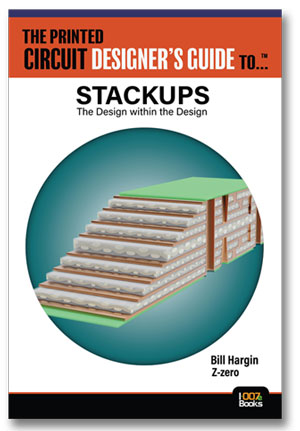
The Printed Circuit Designer’s Guide to... Stackups—The Design within the Design is written by Bill Hargin
Introduction: Mechanical Versus Electrical Worlds
Another book about stackups?
If you’re asking this question, I’d like to know the book you’re thinking of, as I was looking for it a few years back. I have a pretty good PCB signal integrity (SI) library, and I’ve only found one chapter on stackup design so far.
Whenever I talk in person with SI consultants—people who do SI consulting for a living—I ask them, “Of the smoke-jumping projects you’ve been brought in for where there were serious SI problems, how many of those projects have stackup issues?” So far, the only answer I’ve gotten back is, “100 percent.”
The difference between a high-speed PCB design that can be built, and a design that should be built, depends upon the backbone of the design itself: the stackup. The stackup touches every single high-speed signal and yet has had surprisingly little written about it.
In my work, quite a number of PCB stackups cross my desk, and depending on who or what tools were involved in a given design, there are manufacturing parameters that affect both impedance and signal loss that design teams can improve upon.
This book is by no means the last word on the subject, but rather a place to kick off a broader discussion about stackup planning and material selection, to reach the understanding of what I call “the design within the design.”
Share on:


Suggested Items
Cadence, TSMC Collaborate on Wide-Ranging Innovations to Transform System and Semiconductor Design
04/25/2024 | Cadence Design SystemsCadence Design Systems, Inc. and TSMC have extended their longstanding collaboration by announcing a broad range of innovative technology advancements to accelerate design, including developments ranging from 3D-IC and advanced process nodes to design IP and photonics.
Ansys, TSMC Enable a Multiphysics Platform for Optics and Photonics, Addressing Needs of AI, HPC Silicon Systems
04/25/2024 | PRNewswireAnsys announced a collaboration with TSMC on multiphysics software for TSMC's Compact Universal Photonic Engines (COUPE). COUPE is a cutting-edge Silicon Photonics (SiPh) integration system and Co-Packaged Optics platform that mitigates coupling loss while significantly accelerating chip-to-chip and machine-to-machine communication.
Siemens’ Breakthrough Veloce CS Transforms Emulation and Prototyping with Three Novel Products
04/24/2024 | Siemens Digital Industries SoftwareSiemens Digital Industries Software launched the Veloce™ CS hardware-assisted verification and validation system. In a first for the EDA (Electronic Design Automation) industry, Veloce CS incorporates hardware emulation, enterprise prototyping and software prototyping and is built on two highly advanced integrated circuits (ICs) – Siemens’ new, purpose-built Crystal accelerator chip for emulation and the AMD Versal™ Premium VP1902 FPGA adaptive SoC (System-on-a-chip) for enterprise and software prototyping.
Listen Up! The Intricacies of PCB Drilling Detailed in New Podcast Episode
04/25/2024 | I-Connect007In episode 5 of the podcast series, On the Line With: Designing for Reality, Nolan Johnson and Matt Stevenson continue down the manufacturing process, this time focusing on the post-lamination drilling process for PCBs. Matt and Nolan delve into the intricacies of the PCB drilling process, highlighting the importance of hole quality, drill parameters, and design optimization to ensure smooth manufacturing. The conversation covers topics such as drill bit sizes, aspect ratios, vias, challenges in drilling, and ways to enhance efficiency in the drilling department.
Elevating PCB Design Engineering With IPC Programs
04/24/2024 | Cory Blaylock, IPCIn a monumental stride for the electronics manufacturing industry, IPC has successfully championed the recognition of the PCB Design Engineer as an official occupation by the U.S. Department of Labor (DOL). This pivotal achievement not only underscores the critical role of PCB design engineers within the technology landscape, but also marks the beginning of a transformative journey toward nurturing a robust, skilled workforce ready to propel our industry into the future.