-

- News
- Books
Featured Books
- smt007 Magazine
Latest Issues
Current Issue
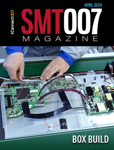
Box Build
One trend is to add box build and final assembly to your product offering. In this issue, we explore the opportunities and risks of adding system assembly to your service portfolio.

IPC APEX EXPO 2024 Pre-show
This month’s issue devotes its pages to a comprehensive preview of the IPC APEX EXPO 2024 event. Whether your role is technical or business, if you're new-to-the-industry or seasoned veteran, you'll find value throughout this program.

Boost Your Sales
Every part of your business can be evaluated as a process, including your sales funnel. Optimizing your selling process requires a coordinated effort between marketing and sales. In this issue, industry experts in marketing and sales offer their best advice on how to boost your sales efforts.
- Articles
- Columns
Search Console
- Links
- Events
||| MENU - smt007 Magazine
Estimated reading time: 1 minute
Tin Whiskers, Part 5: Impact of Testing Conditions
In this installment of the tin whisker series, we'll take a look at the impact of testing conditions, and follow-up with this statement from Part 4: “…all-encompassing tests to confirm or deny the culprits for tin whiskers are prohibitively costly and time-consuming…”
The JEDEC Solid State Technology Association (formerly known as the Joint Electron Device Engineering Council) has published several documents that address and/or are related to the testing of tin whiskers, which are good guidelines with which to start.
- JEDEC Standard No. 201: Environmental Acceptance requirements for Tin Whisker Susceptibility of Tin and Tin Alloy Surface Finishes.
- JEDEC Standard No. 22A12: Measuring Whisker Growth on Tin and Tin Alloy Surface Finishes.
- JEDEC Standard No. 22-A104D: Temperature Cycling.
Primarily, three sets of testing conditions are included in the JEDEC documents: ambient temperature storage, elevated temperature storage and temperature cycling, with the following parameters:
Room Temperature Humidity Storage
30 ± 2°C and 60 ± 3% RH
(1,000 hrs interval inspection/3,000 to 4,000 hours total duration)
Temperature Humidity Unbiased
60 ± 5°C and 87 + 3/-2% RH
(1,000 hours interval inspection/3,000 to 4,000 hours total duration)
Temperature Cycling
Lower end temperature: -55 to -40 (+0/-10)°C
Higher end temperature: +85 (+10/-0)°C
(500 cycles inspection /1,000 to 1,500 cycles duration/air to air/5 to 10 minute soak/three cycles per hour)
Read the full column here.
Editor's Note: This column originally appeared in the May 2014 issue of SMT Magazine.
More Columns from SMT Perspectives and Prospects
SMT Prospects and Perspectives: AI Opportunities, Challenges, and Possibilities, Part 1SMT Perspectives and Prospects: Critical Materials—A Compelling Case, Part 3
SMT Prospects and Perspectives: AI—A Prelude to Opportunities, Challenges and Possibilities
SMT Perspectives and Prospects: Pearls of Wisdom
SMT Perspectives and Prospects: The Role of Bismuth (Bi) in Electronics, Part 7: A Case Study in Fillet-Lifting
SMT Perspectives & Prospects: Creating a Better World Through Engineering
SMT Perspectives and Prospects: Cybersecurity Requires an Active Approach
SMT Perspectives and Prospects: In Search of Wisdom


