


 It’s Only Common Sense: OCCAM—the Time Is Now
 Marcy's Musings: The Growing Industry
 Dan’s Biz Bookshelf: Seeing the How
Printing PCBs…In Your Office!
March 3, 2016 | Barry Matties, I-Connect007Estimated reading time: 1 minute
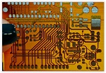
The days of producing a PCB prototype with a 3D printer may not be as distant as you think. I spoke with Simon Fried of Nano Dimension about how 3D printing is becoming a reality, and how this disruptive technology will change the way designers produce rapid prototypes.
Barry Matties: Why don’t you first tell us a little bit about what Nano Dimension does?
Simon Fried: Nano Dimension is a company that is merging the worlds of printed electronics and 3D printing. It’s taking printed electronics, which was a 2D space, putting conductor materials down onto films, and adding that additional material so that you can start building multi-layered circuits. What we’ve developed is a 3D printer that prints multi-layered PCBs right on your desktop in an overnight process.
Matties: Obviously you’re targeting the prototype market—people who just want to produce working prototypes in their office.
Fried: Absolutely. This is for that engineer who’s developing a PCB who needs to do rapid development, quick iterations, has a broad range of different PCBs, and can adapt on the fly to the developments as the development process progresses. It minimizes the risk of changing the PCB design. It allows you perhaps to be more innovative because you’re not going to have to sit around waiting to find out if that great idea you just had is actually going to work. It saves you time, it’ll save you money, but it will also change the way that people work when they’re developing PCBs. It’ll allow you to do things that you otherwise wouldn’t. If you compare that to the way 3D printing affected the prototyping of other objects, like engineering and design, what’s happened in those spaces once 3D printing arrived is they did significantly more prototyping. They found that at the end they were getting better products more rapidly because exploration and innovation became that much easier.
Editor's Note: This article originally appeared in the February 2016 issue of The PCB Magazine.
Share on:


Suggested Items
KIC’s Miles Moreau to Present Profiling Basics and Best Practices at SMTA Wisconsin Chapter PCBA Profile Workshop
01/25/2024 | KICKIC, a renowned pioneer in thermal process and temperature measurement solutions for electronics manufacturing, announces that Miles Moreau, General Manager, will be a featured speaker at the SMTA Wisconsin Chapter In-Person PCBA Profile Workshop.
The Drive Toward UHDI and Substrates
09/20/2023 | I-Connect007 Editorial TeamPanasonic’s Darren Hitchcock spoke with the I-Connect007 Editorial Team on the complexities of moving toward ultra HDI manufacturing. As we learn in this conversation, the number of shifting constraints relative to traditional PCB fabrication is quite large and can sometimes conflict with each other.
Standard Of Excellence: The Products of the Future
09/19/2023 | Anaya Vardya -- Column: Standard of ExcellenceIn my last column, I discussed cutting-edge innovations in printed circuit board technology, focusing on innovative trends in ultra HDI, embedded passives and components, green PCBs, and advanced substrate materials. This month, I’m following up with the products these new PCB technologies are destined for. Why do we need all these new technologies?
Experience ViTrox's State-of-the-Art Offerings at SMTA Guadalajara 2023 Presented by Sales Channel Partner—SMTo Engineering
09/18/2023 | ViTroxViTrox, which aims to be the world’s most trusted technology company, is excited to announce that our trusted Sales Channel Partner (SCP) in Mexico, SMTo Engineering, S.A. de C.V., will be participating in SMTA Guadalajara Expo & Tech Forum. They will be exhibiting in Booth #911 from the 25th to the 26th of October 2023, at the Expo Guadalajara in Jalisco, Mexico.
Intel Unveils Industry-Leading Glass Substrates to Meet Demand for More Powerful Compute
09/18/2023 | IntelIntel announced one of the industry’s first glass substrates for next-generation advanced packaging, planned for the latter part of this decade.