


 It’s Only Common Sense: OCCAM—the Time Is Now
 Marcy's Musings: The Growing Industry
 Dan’s Biz Bookshelf: Seeing the How
MKS Sees Strong Early Market Adoption in Asia for its Newest HDI PCB Laser Manufacturing Solution
September 2, 2020 | MKS Instruments, Inc.Estimated reading time: 2 minutes
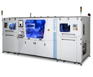
MKS Instruments, Inc., a global provider of technologies that enable advanced processes and improve productivity, announced that Meiko Electronics Co. Japan has purchased multiple ESI® Geode™ Systems to enhance its high-volume HDI PCB manufacturing capability. The recently released CO2-laser-based systems will be deployed at Meiko’s high-end manufacturing facility in Vietnam.
“We are pleased with the market adoption of the Geode system,” said MKS President and CEO John T.C. Lee. “Geode is well-positioned to take advantage of the growing market for HDI PCB processing solutions, as electronics manufacturers continue the path of miniaturization in order to meet the demand for smaller and more capable devices.”
The Geode system delivers many benefits for high-end applications, such as 5G. According to Atsushi Sakate, Executive Officer, General Manager of Production at Meiko,
“Beyond the Geode system’s higher drilling throughput and accuracy, the system’s smaller footprint and lighter weight enables us to plan capacity expansion with much more flexibility. Add to this the broad range of applications and materials that Geode can process, and the decision is clear.”
Developed by MKS’ Equipment & Solutions Division, already a market leader in flex PCB laser drilling solutions, the Geode system is optimized to process the rigid HDI PCBs and package substrates widely used in consumer electronics, such as smartphones and other handheld devices. Building on MKS’ technology leadership in laser processing for flexible printed circuits, Geode’s new CO2 laser technology and control capabilities deliver breakthrough performance. Its superior throughput, refined power control and small system footprint meet the needs of high-volume PCB manufacturers. Learn more about the ESI Geode System at www.esi.com.
About MKS Instruments
MKS Instruments, Inc. is a global provider of instruments, systems, subsystems and process control solutions that measure, monitor, deliver, analyze, power and control critical parameters of advanced manufacturing processes to improve process performance and productivity for our customers. Our products are derived from our core competencies in pressure measurement and control, flow measurement and control, gas and vapor delivery, gas composition analysis, electronic control technology, reactive gas generation and delivery, power generation and delivery, vacuum technology, lasers, photonics, optics, precision motion control, vibration control and laser-based manufacturing systems solutions. We also provide services relating to the maintenance and repair of our products, installation services and training. Our primary served markets include semiconductor, industrial technologies, life and health sciences, research and defense. Additional information can be found at www.mksinst.com.
About the ESI Brand
ESI® is a brand within the MKS Instruments Equipment & Solutions Division. The ESI portfolio consists of laser-based micro manufacturing systems and component test systems that are used worldwide by manufacturers in the electronics industry to process the materials and components that are an integral part of the electronic devices and systems in use today. Leveraging over 40 years of laser-material interaction expertise and applied laser technology, ESI solutions enable customers to optimize production by providing more control, greater application flexibility and more precise processing of a wide range of materials. The result is higher production quality, increased throughput and higher back-end yields at a lower total cost-of-ownership. Additional information can be found at www.esi.com .
Share on:


Suggested Items
Real Time with… IPC APEX EXPO 2024: Tools, Training, and Trends in Manufacturing Engineering
04/25/2024 | Real Time with...IPC APEX EXPOGuest Editor Kelly Dack and Product Specialist Erik Bateham of Polar Instruments discuss Polar's latest technology, including their role in aiding manufacturing engineers. They highlight the advanced capabilities of Polar's tools and the critical role of signal integrity analysis, as well as the importance of accurate modeling in board manufacturing. Polar's unique training approach and demonstration contact details are also explored.
TTM Celebrates the Grand Opening of Its First Manufacturing Facility in Penang
04/25/2024 | TTM Technologies, Inc.TTM Technologies, Inc., a leading global manufacturer of technology solutions including mission systems, radio frequency (RF) components and RF microwave/microelectronic assemblies, and quick-turn and technologically advanced printed circuit boards (PCBs), officially opened its first manufacturing plant in Penang, Malaysia with an investment of USD200 million (approximately RM958 million).
Listen Up! The Intricacies of PCB Drilling Detailed in New Podcast Episode
04/25/2024 | I-Connect007In episode 5 of the podcast series, On the Line With: Designing for Reality, Nolan Johnson and Matt Stevenson continue down the manufacturing process, this time focusing on the post-lamination drilling process for PCBs. Matt and Nolan delve into the intricacies of the PCB drilling process, highlighting the importance of hole quality, drill parameters, and design optimization to ensure smooth manufacturing. The conversation covers topics such as drill bit sizes, aspect ratios, vias, challenges in drilling, and ways to enhance efficiency in the drilling department.
Elevating PCB Design Engineering With IPC Programs
04/24/2024 | Cory Blaylock, IPCIn a monumental stride for the electronics manufacturing industry, IPC has successfully championed the recognition of the PCB Design Engineer as an official occupation by the U.S. Department of Labor (DOL). This pivotal achievement not only underscores the critical role of PCB design engineers within the technology landscape, but also marks the beginning of a transformative journey toward nurturing a robust, skilled workforce ready to propel our industry into the future.
Fujitsu, METRON Collaborate to Drive ESG Success
04/24/2024 | JCN NewswireFujitsu Limited and METRON SAS, a French cleantech company specializing in energy management solutions for industrial decarbonization, today announced a strategic initiative to contribute to the realization of carbon neutrality in the manufacturing industry.