


 Marcy's Musings: The Growing Industry
 It’s Only Common Sense: Here’s What To Do After IPC APEX EXPO 2024
 Dan’s Biz Bookshelf: Seeing the How
3D Printing With Metals
June 11, 2015 | University of TwenteEstimated reading time: 2 minutes
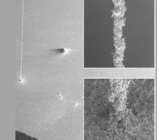
A team of researchers from the University of Twente has found a way to 3D print structures of copper and gold, by stacking microscopically small metal droplets. These droplets are made by melting a thin metal film using a pulsed laser. Their work is published on Advanced Materials.
3D printing is a rapidly advancing field, that is sometimes referred to as the 'new cornerstone of the manufacturing industry'. However, at present, 3D printing is mostly limited to plastics. If metals could be used for 3D printing as well, this would open a wide new range of possibilities. Metals conduct electricity and heat very well, and they're very robust. Therefore, 3D printing in metals would allow manufacturing of entirely new devices and components, such as small cooling elements or connections between stacked chips in smartphones.
However, metals melt at a high temperature. This makes controlled deposition of metal droplets highly challenging. Thermally robust nozzles are required to process liquid metals, but these are hardly available. For small structures in particular (from 100 nanometres to 10 micrometres) no good solutions for this problem existed yet.
Researchers from FOM and the University of Twente now made a major step towards high-resolution metal printing. They used laser light to melt copper and gold into micrometre-sized droplets and deposited these in a controlled manner. In this method, a pulsed laser is focused on a thin metal film. that locally melts and deforms into a flying drop. The researchers then carefully position this drop onto a substrate. By repeating the process, a 3D structure is made. For example, the researchers stacked thousands of drops to form micro-pillars with a height of 2 millimetres and a diameter of 5 micrometres. They also printed vertical electrodes in a cavity, as well as lines of copper. In effect, virtually any shape can be printed by smartly choosing the location of the drop impact.
High Energy
In this study, the researchers used a surprisingly high laser energy in comparison to earlier work, to increase the impact velocity of the metal droplets. When these fast droplets impact onto the substrate, they deform into a disk shape and solidify in that form. The disk shape is essential for a sturdy 3D print: it allows the researchers to firmly stack the droplets on top of each other. In previous attempts, physicists used low laser energies. This allowed them to print smaller drops, but the drops stayed spherical, which meant that a stack of solidified droplets was less stable.
In their article, the researchers explain which speed is required to achieve the desired drop shape. They had previously predicted this speed for different laser energies and materials. This means that the results can be readily translated to other metals as well.
One remaining problem is that the high laser energy also results in droplets landing on the substrate next to the desired location. At present this cannot be prevented. In future work the team will investigate this effect, to enable clean printing with metals, gels, pastas or extremely thick fluids.
Share on:


Suggested Items
Insulectro’s 'Storekeepers' Extend Their Welcome to Technology Village at IPC APEX EXPO
04/03/2024 | InsulectroInsulectro, the largest distributor of materials for use in the manufacture of PCBs and printed electronics, welcomes attendees to its TECHNOLOGY VILLAGE during this year’s IPC APEX EXPO at the Anaheim Convention Center, April 9-11, 2024.
ENNOVI Introduces a New Flexible Circuit Production Process for Low Voltage Connectivity in EV Battery Cell Contacting Systems
04/03/2024 | PRNewswireENNOVI, a mobility electrification solutions partner, introduces a more advanced and sustainable way of producing flexible circuits for low voltage signals in electric vehicle (EV) battery cell contacting systems.
Heavy Copper PCBs: Bridging the Gap Between Design and Fabrication, Part 1
04/01/2024 | Yash Sutariya, Saturn Electronics ServicesThey call me Sparky. This is due to my talent for getting shocked by a variety of voltages and because I cannot seem to keep my hands out of power control cabinets. While I do not have the time to throw the knife switch to the off position, that doesn’t stop me from sticking screwdrivers into the fuse boxes. In all honesty, I’m lucky to be alive. Fortunately, I also have a talent for building high-voltage heavy copper circuit boards. Since this is where I spend most of my time, I can guide you through some potential design for manufacturability (DFM) hazards you may encounter with heavy copper design.
Trouble in Your Tank: Supporting IC Substrates and Advanced Packaging, Part 5
03/19/2024 | Michael Carano -- Column: Trouble in Your TankDirect metallization systems based on conductive graphite or carbon dispersion are quickly gaining acceptance worldwide. Indeed, the environmental and productivity gains one can achieve with these processes are outstanding. In today’s highly competitive and litigious environment, direct metallization reduces costs associated with compliance, waste treatment, and legal issues related to chemical exposure. What makes these processes leaders in the direct metallization space?
AT&S Shines with Purest Copper on World Recycling Day
03/18/2024 | AT&SThe Styrian microelectronics specialist AT&S is taking World Recycling Day as an opportunity to review the progress that has been made in recent months at its sites around the world in terms of the efficient use of resources: