


 Global Sourcing Spotlight: Golf, Friedman, and the Benefits of Global Sourcing
 Nolan’s Notes: Coming to Terms With AI
 The Knowledge Base: A CM’s Perspective on Box Build Practices
Two Prevalent Rework Heating Methods--Which One is Best?
November 7, 2017 | Bob Wettermann, BEST Inc.Estimated reading time: 4 minutes

There are two prevalent heating technologies in use throughout most electronic assembly operations for advanced component rework. The first method employs the use of hot air gas to heat up the component through the package—this may or may not include the injection of nitrogen. A second much-used heating technology relies on infrared energy. This electromagnetic radiation, safe to the operators, is absorbed by the package, thereby sending the solder into reflow.
Hot Air Rework
A typical hot air rework system employs a heat source and an air source that forces the heated air through a nozzle (Figure 1) configured to the area of interest, which heats up the component to be reworked. There are numerous levels of such a hot air system, including a completely manual, a semi-automatic, and an automatic system, each with its own features.
Why Hot Air?
Hot air convection heating for PCB rework is advantageous for a variety of reasons. The absorption of heat by the component and circuit board is independent of a material’s color or texture. Additionally, inducing nitrogen to the site during component reflow has the advantage of making sure the metallurgical structure of the solder joint is the most reliable. In air-atmosphere rework, an oxide layer forms around the solder sphere as it reflows. Inducing nitrogen during this step displaces the oxygen and limits the oxide layer forming around the molten solder. Finally, a hot air convection system quickly delivers heat energy into thermally massive boards.
Figure 1: Nozzle delivers hot air in and around the package during rework cycle.
While there are many advantages to using a hot air rework system, there are some drawbacks the user needs to be aware of when trying to decide which reflow source to use. First, due to the nature of the hot air source and the ever-decreasing mass of SMT components, solder joints can be disturbed or parts can be skewed during reflow. This is especially true for 0201, μBGA and other micro packages. Secondly, to make sure the hot air blows effectively on the package and not onto the neighboring components, a customized nozzle is required. Too large a gap between the edge of the package and the nozzle and then the neighboring parts will tend to go in to reflow. A poorly-designed nozzle leaves a temperature gradient in the hot air source thereby leading to inconsistent results. In addition, customized nozzles take several weeks to fabricate and are not cost-effective for small quantities. Finally, in many cases the peak temperature will be higher for a hot air profile versus that of a similar IR reflow profile. This may cause parts in the neighboring vicinity to those being reworked to reach their softening point (like plastic-bodied relays and connectors), thereby causing damage to them.
What is IR?
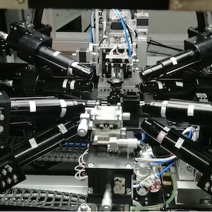
Infrared (IR) technology, the other widely-used heating source for PCB rework, was first introduced into SMT repair equipment in the mid-1980s. An infrared heater is a body transferring energy to a body with a lower temperature through electromagnetic radiation in the infrared spectrum with wavelengths from 780 nm to 1 mm. There are two basic styles of IR technology. The first is medium range IR (Figure 2), which emits the energy and is “blocked” from some areas of the PCB by “shuttering.” The second is a focused IR heat source (Figure 3) in which IR radiation is collimated and directed through a lens system.
Advantage of IR
The IR heating source presents some advantages to the PCB rework process. It is important to realize how passive and gentle the method is and, in fact, at full power the heating effect is so slight that you can hold your hand in the beam for some considerable time before any effect is felt. This makes the technology advantageous for applications where heat-sensitive components found in rework may not be damaged.
Figure 2: Medium IR heating technology for PCB rework.
Page 1 of 2
Share on:


Suggested Items
Connect the Dots: Designing for Reality—The Pre-Manufacturing Process
05/08/2024 | Matt Stevenson -- Column: Connect the DotsI have been working with Nolan Johnson on a podcast series about designing PCBs for the reality of manufacturing. By sharing lessons learned over a long career in the PCB industry, we hope to shorten learning curves and help designers produce better boards with less hassle and rework. Episode 2 deals with the electronic pre-manufacturing process. Moving from CAD (computer-aided design) to CAM (computer-aided manufacturing) is a key step in PCB manufacturing. CAM turns digital designs into instructions that machines can use to actually build the PCB.
AIM Solder Signs Shinil Fl Ltd. as New Distributor for Korea
05/08/2024 | AIM SolderAIM Solder, a leading global manufacturer of solder assembly materials for the electronics industry, is pleased to announce a new distribution partnership with Shinil Fl Ltd., a prominent supplier of technological solutions in the SMT and semiconductor sectors.
Indium Corporation to Showcase HIA Materials at ECTC
05/07/2024 | Indium CorporationAs an industry leader in innovative materials solutions for semiconductor packaging and assembly, Indium Corporation® will feature its advanced products designed to meet the evolving challenges of heterogeneous integration and assembly (HIA) and fine-pitch system-in-package (SiP) applications at the 74th Electronic Components and Technology Conference (ECTC), May 28‒31, in Denver, Colorado.
Indium Corporation Expert to Present on Pb-Free Solder for Die-Attach in Discrete Power Applications
04/30/2024 | Indium CorporationIndium Corporation Product Manager – Semiconductor Dean Payne will present at the Advanced Packaging for Power Electronics conference, hosted by IMAPS, held May 8-9 in Woburn, Massachusetts, USA.
Taiyo Circuit Automation Installs New DP3500 into Fuba Printed Circuits, Tunisia
04/25/2024 | Taiyo Circuit AutomationTaiyo Circuit Automation is proud to be partnered with Fuba Printed Circuits, Tunisia part of the OneTech Group of companies, a leading printed circuit board manufacturer based out of Bizerte, Tunisia, on their first installation of Taiyo Circuit Automation DP3500 coater.