


 American Made Advocacy: What About the Rest of the Technology Stack?
 It’s Only Common Sense: Great Ideas From John Mitchell’s Book on Hiring Habits
 Punching Out: Breaking Out of the Valuation Box
Understanding the Generation of Light-Induced Electrical Current in Atomically Thin Nanomaterials
May 23, 2018 | Brookhaven National LaboratoryEstimated reading time: 5 minutes
Scientists at the Center for Functional Nanomaterials (CFN)—a U.S. Department of Energy (DOE) Office of Science User Facility at Brookhaven National Laboratory—have used an optoelectronic imaging technique to study the electronic behavior of atomically thin nanomaterials exposed to light.
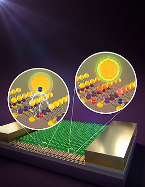
Image caption: A field-effect transistor (the device) containing molybdenum disulfide (stick and balls) doped with core-only quantum dots undergoing charge transfer (left zoom; charge transfer is shown as sparks) and core/shell quantum dots undergoing energy transfer (right zoom; energy transfer is shown as a wave moving from the quantum dots to molybdenum disulfide).
Combined with nanoscale optical imaging, this scanning photocurrent microscopy technique provides a powerful tool for understanding the processes affecting the generation of electrical current (photocurrent) in these materials. Such an understanding is key to improving the performance of solar cells, optical sensors, light-emitting diodes (LEDs), and other optoelectronics—electronic devices that rely on light-matter interactions to convert light into electrical signals or vice versa.
“Anyone who wants to know how light-induced electrical current is distributed across a semiconductor will benefit from this capability,” said CFN materials scientist Mircea Cotlet, co-corresponding author on the May 17 Advanced Functional Materials paper describing the work.
Generating an electrical current
When hit with light, semiconductors (materials that have an electrical resistance in between that of metals and insulators) generate an electric current. Semiconductors that consist of one layer or a few layers of atoms—for example, graphene, which has a single layer of carbon atoms—are of particular interest for next-generation optoelectronics because of their sensitivity to light, which can controllably alter their electrical conductivity and mechanical flexibility. However, the amount of light that atomically thin semiconductors can absorb is limited, thus limiting the materials’ response to light.
To enhance the light-harvesting properties of these two-dimensional (2D) materials, scientists add tiny (10–50 atoms in diameter) semiconducting particles called quantum dots in the layer(s). The resulting “hybrid” nanomaterials not only absorb more light but also have interactions occurring at the interface where the two components meet. Depending on their size and composition, the light-excited quantum dots will transfer either charge or energy to the 2D material. Knowing how these two processes influence the photocurrent response of the hybrid material under different optical and electrical conditions—such as the intensity of the incoming light and applied voltage—is important to designing optoelectronic devices with properties tailored for particular applications.
“Photodetectors sense an extremely low level of light and convert that light into an electrical signal,” explained Cotlet. “On the other hand, photovoltaic devices such as solar cells are made to absorb as much light as possible to produce an electrical current. In order to design a device that operates for photodetection or photovoltaic applications, we need to know which of the two processes—charge or energy transfer—is beneficial.”
(Left to right) Mingxing Li, Mircea Cotlet, Chang-Yong Nam, and Percy Zahl at the new scanning photocurrent microscopy facility at Brookhaven Lab's Center for Functional Nanomaterials.
Page 1 of 2
Share on:


Suggested Items
IPC APEX EXPO: Some Thoughts About Growth
05/16/2024 | Dan Feinberg, I-Connect007After two and a half days of wandering the aisles at IPC APEX EXPO 2024, for the first time, I almost felt like I was exploring CES. There were so many booths and exhibits that I could describe, but I’d like to focus on the growth and huge value of this event, which has expanded well beyond just the growing and impressive exhibit show floor.
The Shaughnessy Report: Unlock Your High-speed Material Constraints
05/15/2024 | Andy Shaughnessy -- Column: The Shaughnessy ReportThe world of PCB materials used to be a fairly simple one. It was divided into two groups: the “traditional” laminates, often called FR-4, and the high-speed laminates developed especially for high-speed PCBs. These were two worlds that usually didn’t collide. But then traditional laminates started getting better, and high-speed designers and design engineers took notice and started to reconsider what FR-4 could be used for.
Breaking High-speed Material Constraints: Design007 Magazine — May 2024
05/14/2024 | I-Connect007 Editorial TeamDo you need specialty materials for your high-speed designs? Maybe not. Improvements in resins mean designers of high-speed boards can sometimes use traditional laminate systems instead of high-speed materials, saving time and money while streamlining the fab process. In the May 2024 issue of Design007 Magazine, our contributors explain how to avoid overconstraining your materials when working with high-speed boards.
Indium Experts to Present at Electronics in Harsh Environments SMTA Conference
05/13/2024 | Indium Corporationndium Corporation Technical Manager for Europe, Africa, and the Middle East, Karthik Vijay, will deliver a technical presentation and Indium Corporation Senior Technologist, Dr. Ronald Lasky, will deliver both a workshop and technical presentation at the Electronics in Harsh Environments SMTA Conference on May 14-16 in Copenhagen, Denmark.
Ansys’ Collaboration with Schrödinger will Accelerate Materials Development with Unprecedented Multiscale Simulation
05/09/2024 | ANSYSAnsys and Schrödinger are collaborating to deliver an ICME approach that bridges the gap between materials discovery and product development.