


 The Right Approach: I Hear the Train A Comin'
 It’s Only Common Sense: OCCAM—the Time Is Now
 Marcy's Musings: The Growing Industry
Ansys Multiphysics Solutions Enable Signoff Verification for Intel 16 Process Node
July 11, 2023 | PRNewswireEstimated reading time: 1 minute
Intel Foundry Services (IFS) certified Ansys multiphysics solutions for signoff verification of advanced integrated circuits (ICs) designed with the Intel 16 silicon manufacturing process. The predictive accuracy of Ansys' power integrity and signal integrity platforms helps designers increase the performance of edge AI, graphic processing, and wireless communication products by avoiding wasteful over-design. The collaboration with IFS validated a seamless electronic design automation (EDA) flow that delivers high productivity for joint customers.
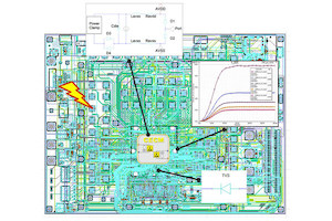
Ansys Redhawk-SC, Ansys Totem, and Ansys PathFinder-SC (pictured) support power integrity, signal integrity, and reliability signoff requirements for the Intel 16 process node
Ansys RedHawk-SC and Ansys Totem are recognized as industry standards for power integrity signoff of digital and analog designs. The solutions' cloud-enabled data infrastructure provides unparalleled capacity to analyze full-chip designs, hierarchically or flat. Ansys PathFinder-SC uses the same elastic compute infrastructure to verify the electrostatic discharge (ESD) protection circuitry found on all chips.
"Ansys and IFS, with a history of close collaboration, are pleased with the broad support of our Intel 16 process including our RF capabilities," said Rahul Goyal, vice president & general manager for Intel's Product & Design Ecosystem Enablement group. "We believe in providing our foundry customers with the widest possible array of industry-leading EDA tools that work in their existing design platforms and that make optimal use of our advanced manufacturing technology."
"Ansys works with leading foundry partners like Intel Foundry Services to address complex multiphysics challenges and meet stringent power, performance, and reliability requirements," said John Lee, vice president and general manager of the electronics, semiconductor, and optics business unit at Ansys. "Ansys' signoff platform helps empower mutual customers to accelerate design convergence with greater confidence thanks to the collaborative work between the companies to ensure silicon predictive accuracy and a smooth user experience."
Share on:


Suggested Items
iNEMI Packaging Tech Topic Series: Role of EDA in Advanced Semiconductor Packaging
04/26/2024 | iNEMIAdvanced semiconductor packaging with heterogenous integration has made on-package integration of multiple chips a crucial part of finding alternatives to transistor scaling. Historically, EDA tools for front-end and back-end design have evolved separately; however, design complexity and the increased number of die-to-die or die-to-substrate interconnections has led to the need for EDA tools that can support integration of overall design planning, implementation, and system analysis in a single cockpit.
Cadence, TSMC Collaborate on Wide-Ranging Innovations to Transform System and Semiconductor Design
04/25/2024 | Cadence Design SystemsCadence Design Systems, Inc. and TSMC have extended their longstanding collaboration by announcing a broad range of innovative technology advancements to accelerate design, including developments ranging from 3D-IC and advanced process nodes to design IP and photonics.
Ansys, TSMC Enable a Multiphysics Platform for Optics and Photonics, Addressing Needs of AI, HPC Silicon Systems
04/25/2024 | PRNewswireAnsys announced a collaboration with TSMC on multiphysics software for TSMC's Compact Universal Photonic Engines (COUPE). COUPE is a cutting-edge Silicon Photonics (SiPh) integration system and Co-Packaged Optics platform that mitigates coupling loss while significantly accelerating chip-to-chip and machine-to-machine communication.
Siemens’ Breakthrough Veloce CS Transforms Emulation and Prototyping with Three Novel Products
04/24/2024 | Siemens Digital Industries SoftwareSiemens Digital Industries Software launched the Veloce™ CS hardware-assisted verification and validation system. In a first for the EDA (Electronic Design Automation) industry, Veloce CS incorporates hardware emulation, enterprise prototyping and software prototyping and is built on two highly advanced integrated circuits (ICs) – Siemens’ new, purpose-built Crystal accelerator chip for emulation and the AMD Versal™ Premium VP1902 FPGA adaptive SoC (System-on-a-chip) for enterprise and software prototyping.
Listen Up! The Intricacies of PCB Drilling Detailed in New Podcast Episode
04/25/2024 | I-Connect007In episode 5 of the podcast series, On the Line With: Designing for Reality, Nolan Johnson and Matt Stevenson continue down the manufacturing process, this time focusing on the post-lamination drilling process for PCBs. Matt and Nolan delve into the intricacies of the PCB drilling process, highlighting the importance of hole quality, drill parameters, and design optimization to ensure smooth manufacturing. The conversation covers topics such as drill bit sizes, aspect ratios, vias, challenges in drilling, and ways to enhance efficiency in the drilling department.