


 Standard of Excellence: Collaboration—The Right Path to Innovation
 Global Sourcing Spotlight: Golf, Friedman, and the Benefits of Global Sourcing
 Nolan’s Notes: Coming to Terms With AI
Acceptance Testing Of Low-Ag Reflow Solder Alloys (Part 2)
August 13, 2015 | K. Troxel, A. Allen, E.E. Benedetto, R. Joshi, Hewlett-Packard Co.Estimated reading time: 7 minutes
In Part 2 of this two-part article series, the authors discussed the test results for low-silver alloys using these solder paste alloy assessment protocols for BGAs and leaded components, and the impact of the alloys on printed circuit assembly process windows.
Test Results and Discussion
Manufacturing DoE Results
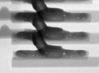
IMC Thickness
Measured on BGA Manufacturing DoE Test Boards (see Figure 1 in Part 1) that were reflowed 3 times with a peak reflow temperature of 250 °C and 120 seconds TAL.
Two BGA body sizes were evaluated [14 mm and 23 mm]. IMC thicknesses for alloys A and B were normally distributed with no significant difference between the large and small BGA. For alloys C and D, greater variability in the large BGA IMC thickness resulted in values significantly different than smaller BGA (as seen in Figure 1 and Table 1).
Figure 1: IMC thickness distribution by Alloy (A-D) and BGA size (large/small)
Table 1: Summary of IMC thicknesses (microns)
Copper Dissolution
This was measured on the BGA Manufacturing DoE Test Boards (see Figure 1 in Part 1) that were reflowed 3 times with a peak reflow temperature of 250°C and 120 seconds TAL.
Cu thickness measurements were made at each solder joint, in the middle of the joint and underneath the soldermask adjacent to the joint. Cu removed was the difference in copper thickness at these two locations. Cu dissolved was determined by subtracting Epsilon (thickness of Cu removed during soldermask etch in the PCB fab process) from the Cu removed values.
Figure 2: Cu dissolution distribution by alloy
Table 2: Summary of Cu dissolved (microns)
The amount of Cu dissolved after soldering was less for the low silver alloys than that for SAC305. The Cu dissolution results were normally distributed for the evaluated alloys but varied with alloy and BGA size (as seen in Figure 2 and Table 2). The Cu dissolution performance varied by BGA size, though not in a consistent fashion. While alloy B showed comparable Cu dissolved values between the 2 BGA sizes, alloy C and D both had more Cu dissolved for the larger BGA while alloy A had greater Cu dissolution values for the small BGA (this could be attributable to bare board Cu characteristics between the different vendors).
Page 1 of 3
Share on:


Suggested Items
Indium Experts to Present on High-Temperature, Lead-Free Solder Paste and High Reliability Liquid Metal Alloys Poster at ECTC
05/16/2024 | Indium CorporationIndium Corporation Research Associate Kyle Aserian will deliver a presentation at the 74th Electronic Components and Technology Conference (ECTC) on May 31, in Denver, Colorado.
Indium Experts to Present at Electronics in Harsh Environments SMTA Conference
05/13/2024 | Indium Corporationndium Corporation Technical Manager for Europe, Africa, and the Middle East, Karthik Vijay, will deliver a technical presentation and Indium Corporation Senior Technologist, Dr. Ronald Lasky, will deliver both a workshop and technical presentation at the Electronics in Harsh Environments SMTA Conference on May 14-16 in Copenhagen, Denmark.
Connect the Dots: Designing for Reality—The Pre-Manufacturing Process
05/08/2024 | Matt Stevenson -- Column: Connect the DotsI have been working with Nolan Johnson on a podcast series about designing PCBs for the reality of manufacturing. By sharing lessons learned over a long career in the PCB industry, we hope to shorten learning curves and help designers produce better boards with less hassle and rework. Episode 2 deals with the electronic pre-manufacturing process. Moving from CAD (computer-aided design) to CAM (computer-aided manufacturing) is a key step in PCB manufacturing. CAM turns digital designs into instructions that machines can use to actually build the PCB.
AIM Solder Signs Shinil Fl Ltd. as New Distributor for Korea
05/08/2024 | AIM SolderAIM Solder, a leading global manufacturer of solder assembly materials for the electronics industry, is pleased to announce a new distribution partnership with Shinil Fl Ltd., a prominent supplier of technological solutions in the SMT and semiconductor sectors.
Indium Corporation to Showcase HIA Materials at ECTC
05/07/2024 | Indium CorporationAs an industry leader in innovative materials solutions for semiconductor packaging and assembly, Indium Corporation® will feature its advanced products designed to meet the evolving challenges of heterogeneous integration and assembly (HIA) and fine-pitch system-in-package (SiP) applications at the 74th Electronic Components and Technology Conference (ECTC), May 28‒31, in Denver, Colorado.