


 Material Insight: The Dielectric Constant of PCB Materials
 American Made Advocacy: What About the Rest of the Technology Stack?
 It’s Only Common Sense: Great Ideas From John Mitchell’s Book on Hiring Habits
Visualizing Atoms of Perovskite Crystals
January 10, 2016 | Okinawa Institute of Science and Technology (OIST) Graduate UniversityEstimated reading time: 2 minutes
Organic-inorganic perovskite materials are key components of the new generation of solar cells. Understanding properties of these materials is important for improving lifetime and quality of solar cells. Researchers from the Energy Materials and Surface Sciences (EMSS) Unit, led by Prof. Yabing Qi, at the Okinawa Institute of Science and Technology Graduate University (OIST) in collaboration with Prof. Youyong Li's group from Soochow University (China) and Prof. Nam-Gyu Park's group from Sungkyunkwan University (Korea) report in the Journal of the American Chemical Society the first atomic resolution study of organic-inorganic perovskite.
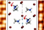
Perovskites are a class of materials with the general chemical formula ABX3. A and B are positive ions bound by negative ions X. Organic-inorganic perovskites used in solar cells are usually methylammonium lead halides (CH3NH3PbX3, where X is bromine, iodine, or chlorine). The OIST scientists used a single crystal of methylammonium lead bromide (CH3NH3PbBr3) to create topographic images of its surface with a scanning tunneling microscope.
This microscope uses a conducting tip that moves across the surface in a manner very similar to a finger moving across a Braille sign. While the bumps in Braille signs are a few millimetres apart, the microscope detects bumps that are more than million times smaller -- atoms and molecules. This is achieved by the quantum tunneling effect -- the ability of an electron to pass through a barrier. The probability of an electron passing between the material surface and the tip depends on the distance between the two. The resulting atomic-resolution topographic images reveal positions and orientations of atoms and molecules, and also provide a detailed look at structural defects in the surface.
"At room temperature atoms and molecules are quite mobile, so we decided to freeze the crystal to almost absolute zero (-269ºC) to get a good picture of its atomic structure," says Dr Robin Ohmann, a member of the EMSS Unit and the first author of the paper. The crystal was cut and studied in a vacuum to avoid contamination of the surface. Dr Ohmann's colleagues from Soochow University calculated atomic structures using principles of quantum physics and then compared them with scanning tunneling microscopy data.
Page 1 of 2
Share on:


Suggested Items
Material Insight: The Dielectric Constant of PCB Materials
05/17/2024 | Dr. Preeya Kuray -- Column: Material InsightIn the world of PCB design, miniaturization can be achieved by using low dielectric constant (Dk) materials. Low Dk materials can allow for a reduction in thickness while maintaining a given trace width, leading to lower transmission loss and higher density circuitry.
IPC APEX EXPO: Some Thoughts About Growth
05/16/2024 | Dan Feinberg, I-Connect007After two and a half days of wandering the aisles at IPC APEX EXPO 2024, for the first time, I almost felt like I was exploring CES. There were so many booths and exhibits that I could describe, but I’d like to focus on the growth and huge value of this event, which has expanded well beyond just the growing and impressive exhibit show floor.
The Shaughnessy Report: Unlock Your High-speed Material Constraints
05/15/2024 | Andy Shaughnessy -- Column: The Shaughnessy ReportThe world of PCB materials used to be a fairly simple one. It was divided into two groups: the “traditional” laminates, often called FR-4, and the high-speed laminates developed especially for high-speed PCBs. These were two worlds that usually didn’t collide. But then traditional laminates started getting better, and high-speed designers and design engineers took notice and started to reconsider what FR-4 could be used for.
Breaking High-speed Material Constraints: Design007 Magazine — May 2024
05/14/2024 | I-Connect007 Editorial TeamDo you need specialty materials for your high-speed designs? Maybe not. Improvements in resins mean designers of high-speed boards can sometimes use traditional laminate systems instead of high-speed materials, saving time and money while streamlining the fab process. In the May 2024 issue of Design007 Magazine, our contributors explain how to avoid overconstraining your materials when working with high-speed boards.
Indium Experts to Present at Electronics in Harsh Environments SMTA Conference
05/13/2024 | Indium Corporationndium Corporation Technical Manager for Europe, Africa, and the Middle East, Karthik Vijay, will deliver a technical presentation and Indium Corporation Senior Technologist, Dr. Ronald Lasky, will deliver both a workshop and technical presentation at the Electronics in Harsh Environments SMTA Conference on May 14-16 in Copenhagen, Denmark.