


 The Chemical Connection: Reducing Etch System Water Usage, Part 2
 It’s Only Common Sense: Nice Guys Really Can Finish First
 The Right Approach: I Hear the Train A Comin'
Scientists Grow a Material Based on Hafnium Oxide for a New Type of Non-volatile Memory
April 15, 2016 | MIPTEstimated reading time: 4 minutes
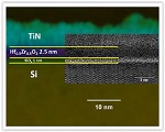
Scientists from MIPT have succeeded in growing ultra-thin (2.5-nanometre) ferroelectric films based on hafnium oxide that could potentially be used to develop non-volatile memory elements called ferroelectric tunnel junctions. The results of the study have been published in the journal ACS Appl. Mater. Interfaces.
Humans are constantly expanding the volume of stored and processed information, which according to statistics is doubling every 1.5 years. To store this information, we need increasing amounts of computer memory, especially non-volatile memory, which stores information even in the event of a power outage. Scientists all over the world are trying to develop faster and more compact storage devices. The ideal would be a “universal” memory device with the speed of RAM, the capacity of a hard drive, and the non-volatility of a flash drive.
There are many known principles that can be used to build memory, but each one has its drawbacks. This is why modern computers and mobile devices have multiple types of memory.
Non-volatile memory based on ferroelectric tunnel junctions is a promising development that has not yet been fully implemented. A ferroelectric is a material that is able to “remember” the direction of an externally applied electric field by the residual polarization charge.
Thin-film ferroelectrics have for a long time been used to make non-volatile memory devices, however it is extremely difficult to miniaturize them in order to achieve high density / storage capacity and, in addition to this, they are made of materials that are “incompatible” with the production processes used in modern microelectronics.
About ten years ago, after ferroelectric properties were demonstrated in ultra-thin single-crystal films of perovskites, an alternative concept for memory devices was proposed – based on the use of the tunnel effect.
Ferroelectrics are generally insulators and do not conduct electricity. However, if the ferroelectric layer is very thin, electrons can “slip” through with a certain probability, thanks to the quantum tunnelling effect. The probability of tunnelling depends on the size and shape of the potential barrier (the energy characteristics of the structure), and the electrons that “pass through” create a tunnel current.
The movement of the electrons in this case is similar to an obstacle course race, and the size of the obstacle is determined by the direction of the polarization vector, which alters the shape of the potential barrier (see image below). Information is written by applying a voltage to the electrodes next to the ultra-thin ferroelectric, and it is read by measuring the tunnelling current.
Fig.1 The concept of a silicon-based ferroelectric tunnel junction. Information is written by applying an external electric field, which changes the direction of the ferroelectric’s polarization vector, and this in turn changes the shape of the potential barrier. Information is read by measuring the tunnel current, which depends on the shape of the barrier. Image courtesy of the authors of the study.
In theory, this type of memory may have an extremely high density, fast reading and writing speeds, and a low level of power consumption. It could become a non-volatile alternative to DRAM (dynamic random-access memory). Modern DRAM has a short retention time (approximately 0.1 seconds), after which the data is either lost or overwritten. Using this type of memory requires a large amount of power. Memory based on ferroelectric tunnel junctions will be able to save power, which is especially important for portable devices that run on batteries. However, until now, all prototypes of devices based on conventional ferroelectrics have not been compatible with silicon technology, which is used in the production of most modern chips.
Page 1 of 2
Share on:


Suggested Items
D Coupon Testing and Data Insights With GreenSource Fabrication
04/17/2024 | Marcy LaRont, PCB007 MagazineMarcy LaRont spoke with Steve Karas of GreenSource Fabrication at the SMTA UHDI conference in March. He presented a case study that GreenSource undertook with a customer on critical via reliability with advanced materials and used the experience to highlight the importance and effectiveness of D coupon testing. He also discussed GreenSource’s approach to data aggregation and a new system they developed to use collected data effectively.
IPC Publishes Comprehensive Strategy to Address Electronics Industry’s Global Workforce Challenge
04/10/2024 | IPCOne of the most difficult and urgent challenges facing the electronics industry is a chronic shortage of adequately skilled workers. Today, IPC unveiled an expansion of its strategy to address the workforce challenges of the U.S. electronics manufacturing industry and called on its more than 3,000 member companies to join in the effort.
UHDI Fundamentals: ASC Sponsors Ultra High Density Interconnect Symposium
03/21/2024 | Anaya Vardya, American Standard CircuitsAmerican Standard Circuits (ASC) is a major sponsor of an upcoming symposium on one of the most talked about new technologies that has come along in quite a while: ultra high density interconnect (UHDI).
onsemi Aligns Business Groups to Expand Product Portfolio and Accelerate Growth
03/13/2024 | onsemionsemi announced the formation of the Analog and Mixed-Signal Group (AMG) which will be led by newly appointed group president, Sudhir Gopalswamy.
Indium Corporation Experts to Present at SEMI THERM
03/07/2024 | Indium CorporationIndium Corporation Global Account Manager and Senior Thermal Technologist Tim Jensen and Product Development Specialist for Thermal Interface Materials Miloš Lazić will present on thermal interface material (TIM) technology at SEMI-THERM, taking place March 25–28 in San Jose, California, U.S.