


 The Chemical Connection: Reducing Etch System Water Usage, Part 2
 It’s Only Common Sense: Nice Guys Really Can Finish First
 The Right Approach: I Hear the Train A Comin'
'Odd Couple' Monolayer Semiconductors Align to Advance Optoelectronics
April 16, 2016 | ORNLEstimated reading time: 3 minutes
Epitaxy, or growing crystalline film layers that are templated by a crystalline substrate, is a mainstay of manufacturing transistors and semiconductors. If the material in one deposited layer is the same as the material in the next layer, it can be energetically favorable for strong bonds to form between the highly ordered, perfectly matched layers. In contrast, trying to layer dissimilar materials is a great challenge if the crystal lattices don’t match up easily. Then, weak van der Waals forces create attraction but don’t form strong bonds between unlike layers.
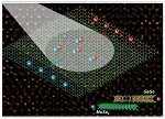
In a study led by the Department of Energy’s Oak Ridge National Laboratory, scientists synthesized a stack of atomically thin monolayers of two lattice-mismatched semiconductors. One, gallium selenide, is a “p-type” semiconductor, rich in charge carriers called “holes.” The other, molybdenum diselenide, is an “n-type” semiconductor, rich in electron charge carriers. Where the two semiconductor layers met, they formed an atomically sharp heterostructure called a p–n junction, which generated a photovoltaic response by separating electron–hole pairs that were generated by light. The achievement of creating this atomically thin solar cell, published in Science Advances, shows the promise of synthesizing mismatched layers to enable new families of functional two-dimensional (2D) materials.
The idea of stacking different materials on top of each other isn’t new by itself. In fact, it is the basis for most electronic devices in use today. But such stacking usually only works when the individual materials have crystal lattices that are very similar, i.e., they have a good “lattice match.” This is where this research breaks new ground by growing high-quality layers of very different 2D materials, broadening the number of materials that can be combined and thus creating a wider range of potential atomically thin electronic devices.
“Because the two layers had such a large lattice mismatch between them, it’s very unexpected that they would grow on each other in an orderly way,” said ORNL’s Xufan Li, lead author of the study. “But it worked.”
The group was the first to show that monolayers of two different types of metal chalcogenides—binary compounds of sulfur, selenium or tellurium with a more electropositive element or radical—having such different lattice constants can be grown together to form a perfectly aligned stacking bilayer. “It’s a new, potential building block for energy-efficient optoelectronics,” Li said.
Upon characterizing their new bilayer building block, the researchers found that the two mismatched layers had self-assembled into a repeating long-range atomic order that could be directly visualized by the Moiré patterns they showed in the electron microscope. “We were surprised that these patterns aligned perfectly,” Li said.
Researchers in ORNL’s Functional Hybrid Nanomaterials group, led by David Geohegan, conducted the study with partners at Vanderbilt University, the University of Utah and Beijing Computational Science Research Center.
“These new 2D mismatched layered heterostructures open the door to novel building blocks for optoelectronic applications,” said senior author Kai Xiao of ORNL. “They can allow us to study new physics properties which cannot be discovered with other 2D heterostructures with matched lattices. They offer potential for a wide range of physical phenomena ranging from interfacial magnetism, superconductivity and Hofstadter’s butterfly effect.”
Li first grew a monolayer of molybdenum diselenide, and then grew a layer of gallium selenide on top. This technique, called “van der Waals epitaxy,” is named for the weak attractive forces that hold dissimilar layers together. “With van der Waals epitaxy, despite big lattice mismatches, you can still grow another layer on the first,” Li said. Using scanning transmission electron microscopy, the team characterized the atomic structure of the materials and revealed the formation of Moiré patterns.
The scientists plan to conduct future studies to explore how the material aligns during the growth process and how material composition influences properties beyond the photovoltaic response. The research advances efforts to incorporate 2D materials into devices.
For many years, layering different compounds with similar lattice cell sizes has been widely studied. Different elements have been incorporated into the compounds to produce a wide range of physical properties related to superconductivity, magnetism and thermoelectrics. But layering 2D compounds having dissimilar lattice cell sizes is virtually unexplored territory.
“We’ve opened the door to exploring all types of mismatched heterostructures,” Li said.
The title of the paper is “Two-dimensional GaSe/MoSe2 misfit bilayer heterojunctions by van der Waals epitaxy.”
Research, including materials synthesis, was supported by the DOE Office of Science. Materials characterization was conducted in part at the Center for Nanophase Materials Sciences, a DOE Office of Science User Facility at ORNL. ORNL Laboratory Directed Research and Development funds supported some of the device measurements in the study.
Share on:


Suggested Items
LQDX Divests Aluminum Soldering Business - Mina™ - to Taiyo America Inc.
05/02/2024 | PRNewswireLQDX, formerly known as Averatek Corp., developer of high-performance materials for advanced semiconductor manufacturing, today announced that it has divested its aluminum soldering business – known as MinaTM – to Taiyo America Inc., a global market leader in advanced electronic materials.
Indium Corporation Expert to Present on Pb-Free Solder for Die-Attach in Discrete Power Applications
04/30/2024 | Indium CorporationIndium Corporation Product Manager – Semiconductor Dean Payne will present at the Advanced Packaging for Power Electronics conference, hosted by IMAPS, held May 8-9 in Woburn, Massachusetts, USA.
Real Time with... IPC APEX EXPO 2024: Adhesive Materials and Equipment Update with Dymax
05/01/2024 | Real Time with...IPC APEX EXPOVirginia Hogan, global business development manager at Dymax, discusses adhesive materials, dispensing and curing equipment, a new, high-reliability conformal coating, and various materials and dispensing methods.
Real Time with... IPC APEX EXPO 2024: Sustainability in the Industry
04/26/2024 | Real Time with...IPC APEX EXPOGuest Editor Henry Crandall and Chris Nash of Indium Corporation discuss the company's 90th anniversary and its focus on sustainability. They focus on the benefits of sustainable materials, their compatibility, and value propositions. The conversation also highlights how Durafuse LT technology's role in reducing reflow temperatures is leading to significant cost and energy savings. Nash also touches on downstream sustainability efforts such as using recycled materials for packaging.
SMC Korea 2024 to Highlight Semiconductor Materials Trends and Innovations on Industry’s Path to $1 Trillion
04/24/2024 | SEMIWith Korea a major consumer of semiconductor materials and advanced materials a key driver of innovation on the industry’s path to $1 trillion, industry leaders and experts will gather at SMC (Strategic Materials Conference) Korea 2024 on May 29 at the Suwon Convention Center in Gyeonggi-do, South Korea to provide insights into the latest materials developments and trends. Registration is open.