


 The Chemical Connection: Reducing Etch System Water Usage, Part 2
 It’s Only Common Sense: Nice Guys Really Can Finish First
 The Right Approach: I Hear the Train A Comin'
Physicists Develop a Cooling System for the Processors of the Future
April 20, 2016 | ACSEstimated reading time: 3 minutes
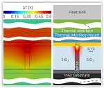
Researchers from MIPT have found a solution to the problem of overheating of active plasmonic components. These components will be essential for high-speed data transfer within the optoelectronic microprocessors of the future, which will be able to function tens of thousands of times faster than the microprocessors currently in use today. In the paper published in ACS Photonics the researchers have demonstrated how to efficiently cool optoelectronic chips using industry-standard heatsinks in spite of high heat generation in active plasmonic components.
The speed of multicore and manycore microprocessors, which are already used in high-performance computer systems, depends not so much on the speed of an individual core, but rather on the time it takes for data to be transferred between the cores. The electrical copper interconnects used in microprocessors today are fundamentally limited in bandwidth, and they cannot be used to maintain the continuing growth of the processor performance. In other words, doubling the number of cores will not double the processing power.
Leading companies in the semiconductor industry, such as IBM, Oracle, Intel, and HP, see the only solution to this problem in switching from electronics to photonics, and they are currently investing billions of dollars into this. Replacing electrons with photons will mean that large amounts of data will be able to be transferred between processor cores almost instantly, which in turn will mean that the processor performance will be nearly proportional to the number of cores. However, due to diffraction, photonic components are not as easy to scale down as electronic components. Their dimensions cannot be smaller than the size approximately equal to the light wavelength (~ 1 micrometer or 1000 nanometers), but transistors will soon be as small as 10 nanometers. This fundamental problem can be solved by switching from bulk waves to surface waves, which are known as surface plasmon polaritons (SPPs). This will enable to confine light on the nanoscale. Along with the leading research centers of industrial companies and the laboratories of leading universities, Russian scientists from the Laboratory of Nanooptics and Plasmonics of MIPT’s Center of Nanoscale Optoelectronics are also making good progress in this field.
Page 1 of 2
Share on:


Suggested Items
The Chemical Connection: Reducing Etch System Water Usage, Part 2
05/02/2024 | Don Ball -- Column: The Chemical ConnectionIn my last column, I reviewed some relatively simple ways to reduce water usage in existing etch systems: cutting down cooling coil water flow, adding chillers to replace plant water for cooling, lowering flow rate nozzles for rinses, etc. This month, I’ll continue with more ways to control water usage in your etcher. Most of these are not easily retrofittable to existing equipment but should be given serious consideration when new equipment is contemplated. With the right combination of add-ons, it is possible to bring the amount of water used in an etch system to almost zero.
Designer’s Notebook: What Designers Need to Know About Manufacturing, Part 2
04/24/2024 | Vern Solberg -- Column: Designer's NotebookThe printed circuit board (PCB) is the primary base element for providing the interconnect platform for mounting and electrically joining electronic components. When assessing PCB design complexity, first consider the component area and board area ratio. If the surface area for the component interface is restricted, it may justify adopting multilayer or multilayer sequential buildup (SBU) PCB fabrication to enable a more efficient sub-surface circuit interconnect.
Insulectro’s 'Storekeepers' Extend Their Welcome to Technology Village at IPC APEX EXPO
04/03/2024 | InsulectroInsulectro, the largest distributor of materials for use in the manufacture of PCBs and printed electronics, welcomes attendees to its TECHNOLOGY VILLAGE during this year’s IPC APEX EXPO at the Anaheim Convention Center, April 9-11, 2024.
ENNOVI Introduces a New Flexible Circuit Production Process for Low Voltage Connectivity in EV Battery Cell Contacting Systems
04/03/2024 | PRNewswireENNOVI, a mobility electrification solutions partner, introduces a more advanced and sustainable way of producing flexible circuits for low voltage signals in electric vehicle (EV) battery cell contacting systems.
Heavy Copper PCBs: Bridging the Gap Between Design and Fabrication, Part 1
04/01/2024 | Yash Sutariya, Saturn Electronics ServicesThey call me Sparky. This is due to my talent for getting shocked by a variety of voltages and because I cannot seem to keep my hands out of power control cabinets. While I do not have the time to throw the knife switch to the off position, that doesn’t stop me from sticking screwdrivers into the fuse boxes. In all honesty, I’m lucky to be alive. Fortunately, I also have a talent for building high-voltage heavy copper circuit boards. Since this is where I spend most of my time, I can guide you through some potential design for manufacturability (DFM) hazards you may encounter with heavy copper design.