


 Dan’s Biz Bookshelf: ‘In Defense of a Liberal Education’
 American Made Advocacy: A Growing Presence in Washington in Turbulent Times


AT&S Tech Enables Evaluation of Fully Integrated GaN-based Multilevel Power Converter
April 25, 2017 | AT&SEstimated reading time: 1 minute
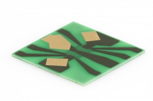
Fraunhofer IAF has developed a fully integrated monolithic multilevel converter in high-volt AlGaN/GaN-on-Si technology. The integrated inverter circuit is designed for maximum voltages of +/- 400 V and currents of 5 A. The multilevel converter on an area of just 2 × 3 mm² comprises four transistors and six diodes. It provides a perfect solution for compact voltage converter applications. It was possible to demonstrate DC/AC inverter operation for American mains voltage. The circuit exhibits minimal dynamic losses at very high frequencies. The excellent switching performance of the multilevel converter was demonstrated with a test setup on the basis of the ECP® technology from AT&S.
A corresponding test setup is necessary in order to evaluate the chip. The packaging of the die constitutes a key factor in this regard. If lateral components are employed, the source, drain and gate pads are on one side and the back of the die is used for heat dissipation. Since the conventional approach with wirebonds imposed restrictions, the second step of the evaluation saw the ECP® technology from AT&S being used. With this technology, the power components – like the multilevel converter – are embedded into the PCB material and can be connected from both sides. The chips are connected directly via copper-plated microvias. This permits low impedance connections and significantly lower inductances compared with wirebond technology. The rear of the die is also connected by means of copper-plated microvias. This ensures excellent heat dissipation.
For more information, click here.
Share on:


Testimonial
"Advertising in PCB007 Magazine has been a great way to showcase our bare board testers to the right audience. The I-Connect007 team makes the process smooth and professional. We’re proud to be featured in such a trusted publication."
Klaus Koziol - atgSuggested Items
Statement from the Global Electronics Association on the July 2025 Tariff on Copper Foil and Electronics-Grade Copper Inputs
07/31/2025 | Global Electronics AssociationWe are disappointed by today’s decision to impose a 50% tariff on imported copper foil and other essential materials critical to electronics manufacturing in the United States.
Considering the Future of Impending Copper Tariffs
07/30/2025 | I-Connect007 Editorial TeamThe Global Electronics Association is alerting industry members that a potential 50% tariff on copper could hit U.S. electronics manufacturers where it hurts.
Connect the Dots: Sequential Lamination in HDI PCB Manufacturing
07/31/2025 | Matt Stevenson -- Column: Connect the DotsAs HDI technology becomes mainstream in high-speed and miniaturized electronics, understanding the PCB manufacturing process can help PCB design engineers create successful, cost-effective designs using advanced technologies. Designs that incorporate blind and buried vias, boards with space constraints, sensitive signal integrity requirements, or internal heat dissipation concerns are often candidates for HDI technology and usually require sequential lamination to satisfy the requirements.
OKI Launches Rigid-Flex PCBs with Embedded Copper Coins Featuring Improved Heat Dissipation for Space Equipment Applications
07/29/2025 | BUSINESS WIREOKI Circuit Technology, the OKI Group’s printed circuit board (PCB) business company, has developed rigid-flex PCBs with embedded copper coins that offer improved heat dissipation for use in rockets and satellite-mounted equipment operating in vacuum environments.
Designers Notebook: Basic PCB Planning Criteria—Establishing Design Constraints
07/22/2025 | Vern Solberg -- Column: Designer's NotebookPrinted circuit board development flows more smoothly when all critical issues are predefined and understood from the start. As a basic planning strategy, the designer must first consider the product performance criteria, then determine the specific industry standards or specifications that the product must meet. Planning also includes a review of all significant issues that may affect the product’s manufacture, performance, reliability, overall quality, and safety.